LITHOGRAPHY BUSINESS GROUP Richard Rogoff

LITHOGRAPHY SYSTEMS GROUP • Headquarters in Wilmington, Massachusetts • More than 400 years of combined lithography experience dating from the 1980s and GCA steppers • Large IP portfolio surrounding Advanced Packaging and Display Lithography • Well developed supply chain poised for growth and technology advancement 2

JETSTEP® SYSTEM THE COMPLETE ADVANCED PACKAGING SYSTEM COVERS ALL APPLICATION SPACE 3 Wafer Wafer Panel Panel Wafer Wafer Panel Wafer

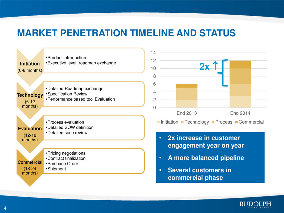
MARKET PENETRATION TIMELINE AND STATUS Initiation (0-6 months) •Product introduction •Executive level roadmap exchange Technology (6-12 months) •Detailed Roadmap exchange •Specification Review •Performance based tool Evaluation Evaluation (12-18 months) •Process evaluation •Detailed SOW definition •Detailed spec review Commercial (18-24 months) •Pricing negotiations •Contract finalization •Purchase Order •Shipment 4 0 2 4 6 8 10 12 14 End 2013 End 2014 Initiation Technology Process Commercial • 2x increase in customer engagement year on year • A more balanced pipeline • Several customers in commercial phase 2x

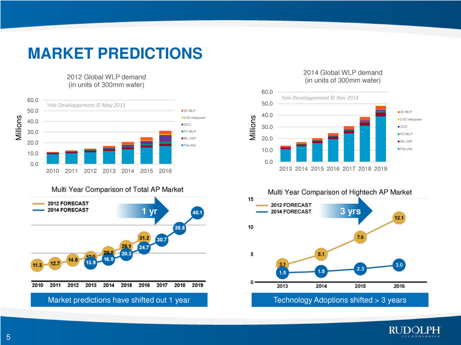
MARKET PREDICTIONS 0.0 10.0 20.0 30.0 40.0 50.0 60.0 2010 2011 2012 2013 2014 2015 2016 2012 Global WLP demand (in units of 300mm wafer) 3D WLP 2.5D interposer 3DIC FO WLP WL CSP Flip-chip Yole Developpement © May 2011 5 0.0 10.0 20.0 30.0 40.0 50.0 60.0 2013 2014 2015 2016 2017 2018 2019 2014 Global WLP demand (in units of 300mm wafer) 3D WLP 2.5D interposer 3DIC FO WLP WL CSP Flip-chip Yole Developpement © Nov 2014 Market predictions have shifted out 1 year Multi Year Comparison of Total AP Market Multi Year Comparison of Hightech AP Market 1 yr Technology Adoptions shifted > 3 years 3 yrs M ill io n s M ill io n s

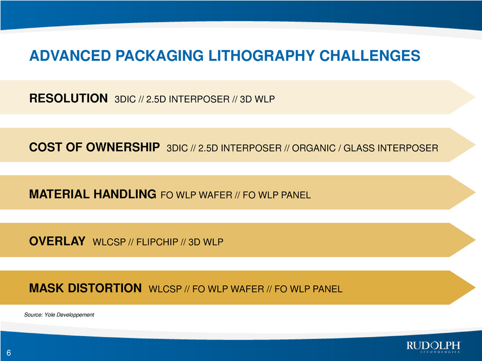
ADVANCED PACKAGING LITHOGRAPHY CHALLENGES 6 Source: Yole Developpement RESOLUTION 3DIC // 2.5D INTERPOSER // 3D WLP COST OF OWNERSHIP 3DIC // 2.5D INTERPOSER // ORGANIC / GLASS INTERPOSER MATERIAL HANDLING FO WLP WAFER // FO WLP PANEL OVERLAY WLCSP // FLIPCHIP // 3D WLP MASK DISTORTION WLCSP // FO WLP WAFER // FO WLP PANEL

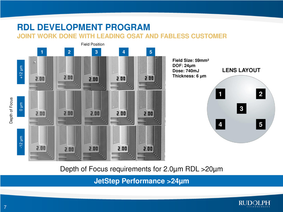
-1 2 μ m 0 μ m + 1 2 μ m 5 2 3 4 1 Dep th o f F o c u s Field Position Field Size: 59mm² DOF: 24μm Dose: 740mJ Thickness: 6 μm 1 3 4 5 2 LENS LAYOUT Depth of Focus requirements for 2.0µm RDL >20µm JetStep Performance >24µm RDL DEVELOPMENT PROGRAM JOINT WORK DONE WITH LEADING OSAT AND FABLESS CUSTOMER 7

75μm Diameter Fabricated using JSR THB-151N at 50μm FT Depth of Focus requirements for Copper Pillar >100µm -60 μm 60 μm 0 μm ELECTROPLATED COPPER PILLAR DEVELOPMENT 8 JetStep Performance >120µm

9 A leading OSAT ran a head to head throughput comparison utilizing live production wafers on a leading 1x stepper and a JetStep W2300 CUSTOMER PROVEN VALUE OF OWNERSHIP JetStep delivers ~20% greater productivity

From FOUP to pre-aligner to stage 10 Loaded on stage, expose and then unload Max Warpage JetStep W2300 -4/+6 mm 1x Competitor +2.5 mm (requires Lens adj) Adapted Front- end Tool +2.5 mm JETSTEP’S INDUSTRY LEADING MATERIAL HANDLER JetStep outperforms all major competitors

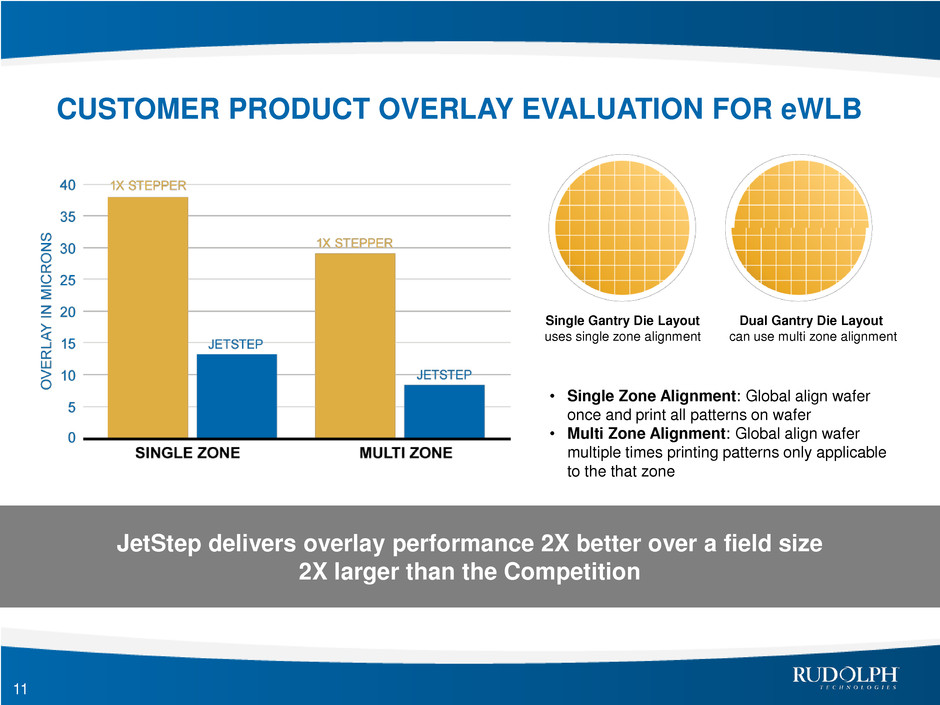
11 • Single Zone Alignment: Global align wafer once and print all patterns on wafer • Multi Zone Alignment: Global align wafer multiple times printing patterns only applicable to the that zone Single Gantry Die Layout uses single zone alignment Dual Gantry Die Layout can use multi zone alignment 1 x S te p p er 1 x S te p p er CUSTOMER PRODUCT OVERLAY EVALUATION FOR eWLB JetStep delivers overlay performance 2X better over a field size 2X larger than the Competition

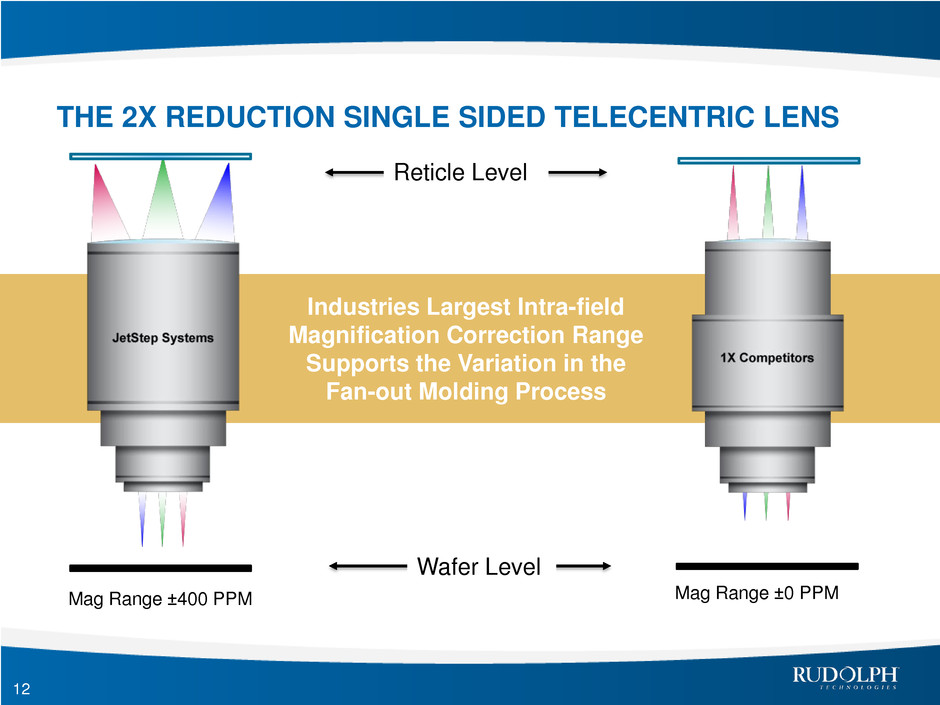
12 THE 2X REDUCTION SINGLE SIDED TELECENTRIC LENS Industries Largest Intra-field Magnification Correction Range Supports the Variation in the Fan-out Molding Process Wafer Level Reticle Level Mag Range ±400 PPM Mag Range ±0 PPM

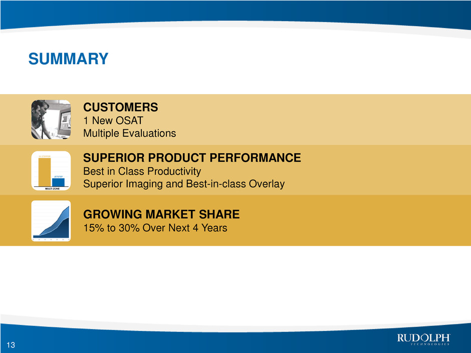
13 SUMMARY CUSTOMERS 1 New OSAT Multiple Evaluations SUPERIOR PRODUCT PERFORMANCE Best in Class Productivity Superior Imaging and Best-in-class Overlay GROWING MARKET SHARE 15% to 30% Over Next 4 Years

THANK YOU
