UNITED STATES
SECURITIES AND EXCHANGE COMMISSION
Washington, D.C. 20549
SCHEDULE 14A
Proxy Statement Pursuant to Section 14(a) of the
Securities Exchange Act of 1934 (Amendment No. )
Filed by the Registrant ¨
Filed by a Party other than the Registrant x
Check the appropriate box:
| ¨ | Preliminary Proxy Statement | |
| ¨ | Confidential, for Use of the Commission Only (as permitted by Rule 14a-6(e)(2)) | |
| ¨ | Definitive Proxy Statement | |
| ¨ | Definitive Additional Materials | |
| x | Soliciting Material under §240.14a-12 | |
SunEdison Semiconductor Limited
(Name of Registrant as Specified In Its Charter)
GlobalWafers Co., Ltd.
(Name of Person(s) Filing Proxy Statement, if other than the Registrant)
Payment of Filing Fee (Check the appropriate box):
| x | No fee required. | |||
| ¨ | Fee computed on table below per Exchange Act Rules 14a-6(i)(1) and 0-11. | |||
| (1) | Title of each class of securities to which transaction applies:
| |||
| (2) | Aggregate number of securities to which transaction applies:
| |||
| (3) | Per unit price or other underlying value of transaction computed pursuant to Exchange Act Rule 0-11 (set forth the amount on which the filing fee is calculated and state how it was determined):
| |||
| (4) | Proposed maximum aggregate value of transaction:
| |||
| (5) | Total fee paid:
| |||
| ¨ | Fee paid previously with preliminary materials. | |||
| ¨ | Check box if any part of the fee is offset as provided by Exchange Act Rule 0-11(a)(2) and identify the filing for which the offsetting fee was paid previously. Identify the previous filing by registration statement number, or the Form or Schedule and the date of its filing. | |||
| (1) | Amount Previously Paid:
| |||
| (2) | Form, Schedule or Registration Statement No.:
| |||
| (3) | Filing Party:
| |||
| (4) | Date Filed:
| |||
 August 18, 2016 GlobalWafers Agreement to Acquire SunEdison Semiconductor |
 Additional Information and Where You Can Find It This communication may be deemed to be solicitation material in respect of the proposed transaction between SunEdison Semiconductor and GlobalWafers. In connection with the proposed transaction, SunEdison Semiconductor will file a proxy statement with the U.S. Securities and Exchange Commission (“SEC”). The proxy statement will be mailed to the shareholders of SunEdison Semiconductor. SHAREHOLDERS OF SUNEDISON SEMICONDUCTOR ARE URGED TO READ THE PROXY STATEMENT WHEN IT BECOMES AVAILABLE AND ANY OTHER DOCUMENTS FILED WITH THE SEC IN CONNECTION WITH THE PROPOSED TRANSACTION OR INCORPORATED BY REFERENCE IN THE PROXY STATEMENT (IF ANY) BECAUSE THEY WILL CONTAIN IMPORTANT INFORMATION. The proxy statement (when it becomes available), and any other documents filed by SunEdison Semiconductor or GlobalWafers with the SEC, may be obtained free of charge at the SEC’s website at www.sec.gov. Shareholders are urged to read the proxy statement and the other relevant materials when they become available before making any decision with respect to the proposed transaction. Certain Information Concerning Participants Each of GlobalWafers, SunEdison Semiconductor and their respective directors and executive officers may be deemed to be participants in the solicitation of proxies from SunEdison Semiconductor shareholders in favor of the proposed transaction. GlobalWafers currently owns approximately 4.9% of the outstanding ordinary shares of SunEdison Semiconductor. Information about GlobalWafers and its directors and executive officers may be found in the Schedule 14A filed by GlobalWafers with the SEC on August 18, 2016. Information about SunEdison Semiconductor’s directors and executive officers and their ownership of SunEdison Semiconductor’s ordinary shares is set forth in its proxy statement for its 2016 Annual General Meeting of Shareholders and its most recent annual report on Form 10-K. Additional information regarding the direct or indirect interests of participants in the solicitation of proxies in connection with the contemplated transactions, by security holdings or otherwise, will be included in the proxy statement and other materials to be filed with the SEC in connection with the transaction. Cautionary Statement Regarding Forward-Looking Information This material contains forward-looking statements. These statements include a belief that the transaction can be closed by the end of the year and expectations by GlobalWafers of the benefits of the transaction. These forward-looking statements are subject to risks and uncertainties. Consequently, actual results and experience may materially differ from those contained in any forward-looking statements. Such risks and uncertainties include the risk that the transaction may not be completed in a timely manner or at all, which may adversely affect SunEdison Semiconductor’s business and the price of its ordinary shares; the failure to obtain SunEdison Semiconductor shareholder approval of the proposed transaction; the possibility that the closing conditions to the transaction may not be satisfied or waived, including that a governmental entity may prohibit, delay or refuse to grant a necessary regulatory approval; delay in closing the transaction or the possibility of non-consummation of the transaction; the potential for regulatory authorities to require divestitures in connection with the proposed transaction; the occurrence of any event that could give rise to termination of the Implementation Agreement; the risk of shareholder litigation that may be instituted in connection with the contemplated transactions; risks related to the diversion of management’s attention from SunEdison Semiconductor’s ongoing business operations; the failure of GlobalWafers to obtain the necessary financing to complete the transaction; the effect of announcement of the transaction on SunEdison Semiconductor’s ability to retain and hire key personnel and maintain relationships with customers, suppliers and other third parties; and difficult global economic and capital markets conditions. Forward-looking statements speak only as of the date they are made. Readers are cautioned not to put undue reliance on forward-looking statements, and GlobalWafers makes no commitment to revise or update any forward-looking statements in order to reflect events or circumstances occurring or existing after the date any forward-looking statement is made. |
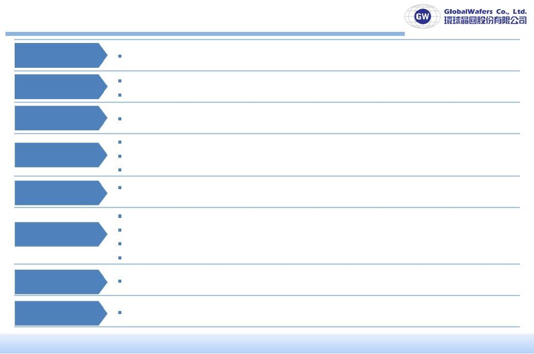
 Agenda 1. Transaction overview 1 2. Overview of the Target 2 3. Strategic rationale 7 4. Q&A 12 |
 Transaction overview |
 100% equity in SunEdison Semiconductor Limited (NASDAQ: SEMI) US$12.00 per SEMI share Represents a transaction value of $683 million including SEMI net debt 1 100% cash consideration 45% premium to last trading day close 2,3 79% premium to 30 day average 2 103% premium to 90 day average 2 Acquisition will be implemented by way of a Scheme of Arrangement under Section 210 of the Companies Act, Chapter 50 of Singapore SEMI shareholder approval U.S. CFIUS Taiwan Investment Commission Antitrust review in the US, Germany and Austria Transaction expected to close by the end of 2016 Acquisition funded using existing cash on hand and committed acquisition financing 1. Equity value based on purchase of basic common shares outstanding and outstanding options and RSUs. 2. Last trading day prior to the announcement was 17 August 2016 3. Close price on the last trading day prior to the announcement was $8.28. Purchase Price Premia Consideration Acquisition method Key conditions to close Timing to close Financing 1 Target Transaction summary |
 Overview of the Target |
 SEMI company history 1959 1962 Developed dislocation-free CZ silicon crystal growth process 1975 Achieved first commercial production of 100mm wafers 1984 Commercialized 200mm wafers 1998 Developed agglomerated defect free ‘Perfect Silicon’ 2009 Began high volume manufacturing of SOI wafers 2013 Deployed diamond wire cutting technology; parent company changed name from MEMC to SunEdison, Inc. 2015 Announced closure of Malaysian Ipoh facility, moved 200mm wafer production to Italy to lower costs / maximize utilization 1965 Developed chemical- mechanical polishing process 1991 Developed 300mm wafers 2011 Qualified wafers for production in 28 nanometer node 2014 Spun off from SunEdison, Inc. in May and listed on NASDAQ 1982 Developed the use of EPI wafers in CMOS applications 2000 Introduced defect- free engineered products ‘MDZ’ & ‘Optia’ Founded as MEMC; headquartered in St. Peters, Missouri 2 2 |
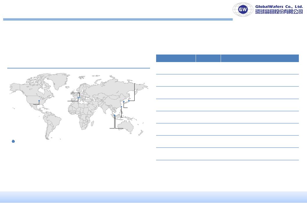 Overview of SEMI Source: Company information. SEMI is a global supplier of SOI and EPI wafers with synergistic/complementary 300mm high volume production with a global manufacturing footprint Utsunomiya, Japan St. Peters, MO Hsinchu, Taiwan Cheonan, South Korea Novara, Italy Merano, Italy Singapore Kuala Lumpur, Malaysia Location Sq. Ft. Product St. Peters, MO 431k 200 / 300mm SOI Merano, Italy 98k Single Crystal Silicon Ingots Novara, Italy 418k 200mm Kuala Lumpur 55k Polished wafers Singapore 3k Business Operations Utsunomiya, Japan 328k 300mm polished and EPI wafers Cheonan, S. Kor. 469k EPI, 200mm, 300mm Hsinchu, Taiwan 558k EPI, 200mm, 300mm Production facilities SEMI Facility 3 |
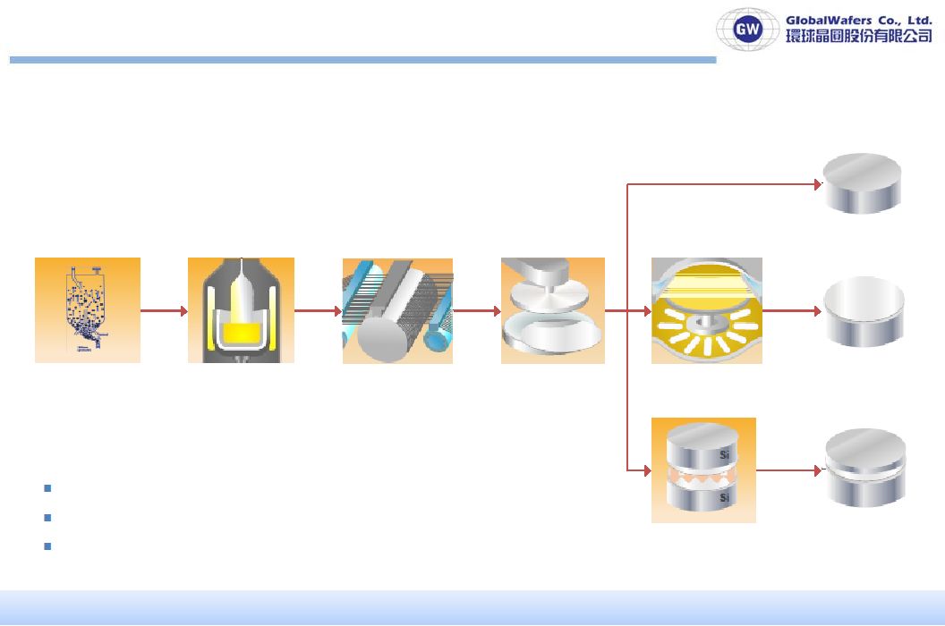 SEMI uses a Unique Advanced Equipment Automation Platform to maximize process capability & productivity; differentiated semi-continuous granular poly based crystal process Manufacturing capability provides new growth platform opportunity Polysilicon Crystal growth Wire saw Wafer polishing Epitaxial deposition Wafer bonding Polished wafers EPI wafers SOI wafers Significantly enhanced EPI throughput through OEE programs One of only 2 fully integrated SOI manufacturers 600+ published and pending patents Source: Company information. 4 |
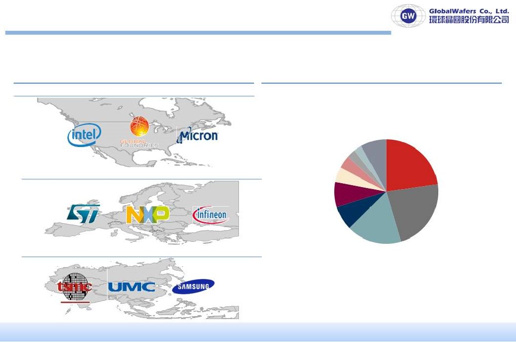 Source: Company information 1. Based on 2015A Revenue of $778 million. SEMI serves all of the top 25 customers in the semiconductor industry North America Europe Asia Customers 5 Taiwan 23% Korea 23`% USA 17% Germany 8% China 8% Italy 5% France 4% Ned. 3% Malaysia 2% Other 8% Revenue by geography 1 Top customers |
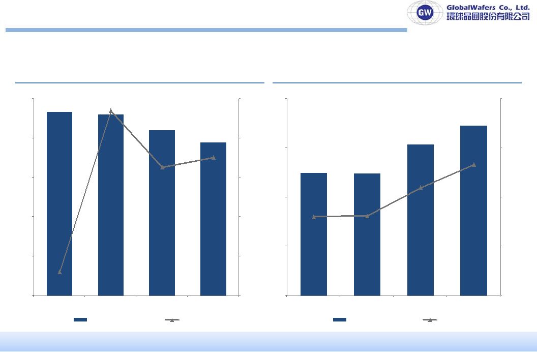 Financial highlights Source: Company information. Although the overall volumes are shrinking due to softness in chip demand, SEMI has focused on optimizing operations and materials costs to drive EBITDA margin Revenue EBITDA 934.2 920.6 840.1 777.5 (22.0%) (1.5%) (8.7%) (7.5%) (25.0%) (20.0%) (15.0%) (10.0%) (5.0%) 0.0% 0 200 400 600 800 1,000 2012A 2013A 2014A 2015A $m Revenue % Growth 74.9 74.6 92.3 103.6 8.0% 8.1% 11.0% 13.3% 0.0% 5.0% 10.0% 15.0% 20.0% 0 30 60 90 120 2012A 2013A 2014A 2015A $m EBITDA % Margin 6 |
 Strategic rationale |
 A combination of GWC and SEMI provides a unique opportunity to expand customer base, enhance product offerings and production capabilities and increase scale Strategic rationale for the transaction Expand production capability with opportunity to optimize production facilities 2 Diversify customer base and revenue base 1 Achieve greater operating scale by creating the 3 rd largest semiconductor silicon wafer manufacturer globally 3 7 Potential for meaningful synergy creation 4 |
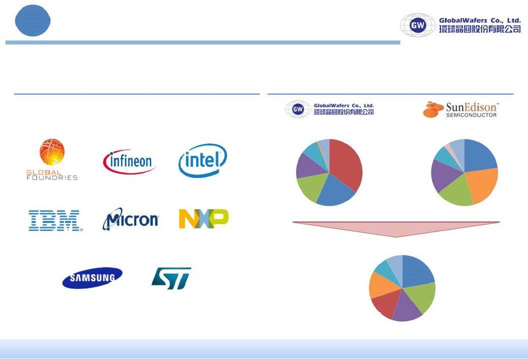 Source: Company information. GWC will gain access to the new customers and more diversified revenue base Customer diversification introduces new customer base Combination will diversify geographic revenue base Diversify customer base and revenue base 1 8 Taiwan 23% S. Korea 23% Europe 19% USA 17% China 8% Malaysia 2% Other 8% Taiwan 22% Europe 17% USA 16% Japan 15% S. Korea 14% China 8% Other 8% Japan 35% Taiwan 21% Europe 15% USA 13% China 9% S. Korea 1% Other 6% |
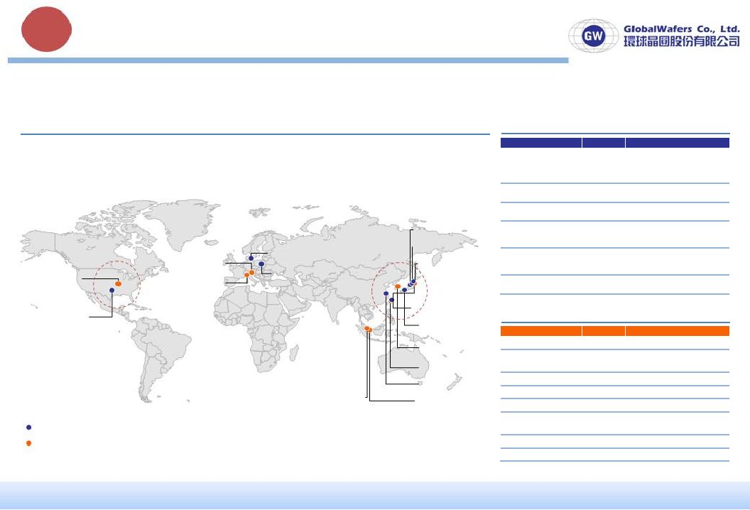 Production facilities overview GWC facilities SEMI facilities 1 Source: Company information. SEMI’s global manufacturing presence would meaningfully expand GWC’s production capabilities while also providing opportunities for cost savings through facility optimization GWC Facility SEMI Facility St. Peters, MO Novara, Italy Merano, Italy Singapore Kuala Lumpur, Malaysia Sherman, Texas Kunshan, China Niigata, Japan Tokuyama, Japan Oguni, Japan Location Sq. Ft. Product St. Peters, MO 431k 200 / 300mm SOI Merano, Italy 98k Single Crystal Silicon Ingots Novara, Italy 200k 200mm Kuala Lumpur 55k Polished wafers Singapore 3k Business Operations Utsunomiya, Japan 328k 300mm polished and EPI wafers Cheonan, S. Kor. 469k EPI, 200mm, 300mm Hsinchu, Taiwan 558k EPI, 200mm, 300mm Location Sq. Ft. Product Hsinchu, Taiwan 101k 75mm–200mm Ingots; 75mm– 150mm wafers; Heavily-doped / Lapped / Etched / Polished / Diffused wafers Kunshan, China 151k 75mm–200mm wafers; Heavily- doped wafers Texas, USA 16k 125mm–200mm wafers; EPI wafers Japan (4 Fabs) 979k 125mm–300mm wafers; Light & Heavily-doped wafers; Annealed / Diffused / SOI / EPI wafers Copenhagen, Denmark 61k 150mm-200mm wafers; ultrapure silicon based on FZ technology Warsaw, Poland 8k CZ/FZ wafering and polishing; EPI on CZ wafers Utsunomiya, Japan Hsinchu, Taiwan Cheonan, South Korea Sekikawa, Japan Expand production capability with opportunity to optimize production facilities Warsaw, Poland Copenhagen, Denmark 9 2 |
 2015A wafer manufacturing worldwide revenue Source: CapitalIQ, company information. Note: Assumes USD/TWD exchange rate of 32.8045. 1. Includes Topsil revenue. The combination of GWC with SEMI will result in the 3rd largest semiconductor silicon wafer manufacturer globally (the largest among non-Japanese manufacturers) with significant additional scale relative to peers Achieve greater operating scale by creating the 3rd largest silicon wafer manufacturer globally 10 3 6% 27% 26% 17% 13% 10% 9% 7% 3% 2% 1% 1% 0% 10% 20% 30% 1% 1 1 |
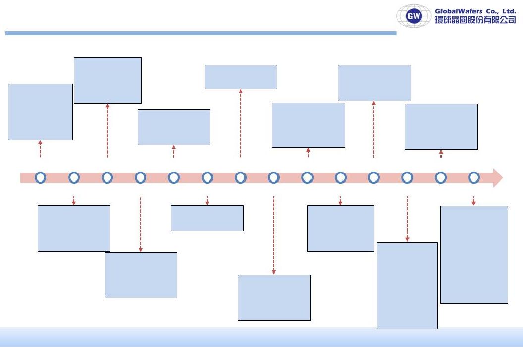
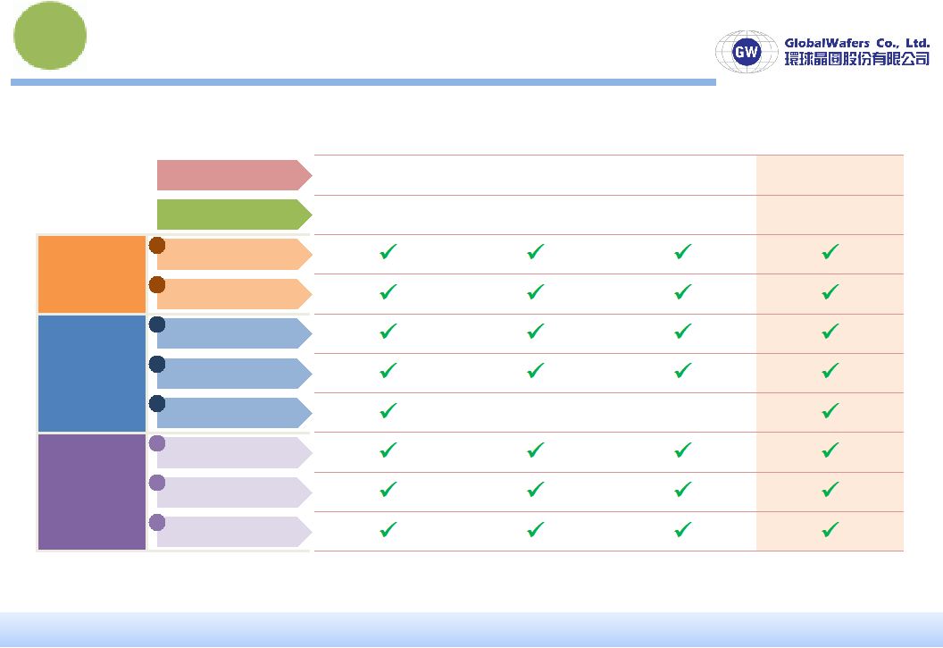 GWC track record and potential synergy with SEMI GWC targets post-tax synergies of approximately US$50 million through the acquisition of SEMI April 2008 August 2011 May 2016 August 2016 Globitech Covalent Materials (Silicon Wafer Business) Topsil SEMI Note: Cross selling includes cross selling new products to each other’s customers. Synergies and commentary are as per each company’s announcements in press releases and filings. Revenue Synergies Cost Synergies Capex / R&D Cross Selling Complementary Geographic Mix Procurement / Enhanced Buyer Power Corporate SG&A / Personnel Expense Debt Financing Integrated Manufacturing New Technology Introduction Integrated R&D 1 2 3 4 5 6 7 8 Completion / Announcement Date Target 11 4 |
 Q&A |