| Name of Partner | Category of Partner | Capital Contributions (RMB 10,000 Yuan) | Capital Proportion (%) |
| Shanghai Shangguo Investment Asset Management Co., Ltd. | Limited Partner | 1,400 | 60.26 |
| Shanghai Jiushen Equity Investment Fund Partnership Enterprise (L.P.) | Limited Partner | 800 | 34.43 |
| FAN LIU | Limited Partner | 100 | 4.30 |
| Shanghai Jiuyou Chuangu Investment Management Co., Ltd. | General Partner | 23.23 | 1.00 |
| Total | | 2,323.23 | 100.00 |
(3) Basic Information of the General Partner
| Name | Shanghai Jiuyou Chuangu Investment Management Co., Ltd. |
| Domicile | Room 08, 5/F, No.2 Office Building, Lane 180, Zhangheng Road, China (Shanghai) Pilot Free Trade Zone |
Date of Establishment | January 16, 2013 |
Uniform Social Credit Code | 91310115060900342P |
Legal Representative | XIAOLONG LIU |
| Registered Capital | RMB 5 million Yuan |
| Business Scope | Industrial investment; investment management; investment consultancy; business consultancy, enterprise management consultancy (brokerage services are not included in the above consultancy services); asset management (For projects subject to any approval in accordance with laws, business activities may be carried out only after such approval of relevant authorities has been obtained) |
12. Runguang Investment
(1) Basic Information
| Name | Hefei Runguang Equity Investment Partnership (L.P.) |
| Domicile | Room 560, Fund Tower, Building E1, Innovation Industrial Park Phase II, No.2800 Innovation Avenue, High-tech Zone, Hefei City |
Uniform Social Credit Code | 91340100MA2TER55XC |
| Executive Partner | Huaxin Yuanchuang (Qingdao) Capital Management Co., Ltd. |
| Registered Capital | RMB 100 million Yuan |
| Type of Enterprise | Limited Partnership |
| Business Scope | Using self-owned funds to make equity investment; enterprise management consultancy services. (being prohibited from engaging in financial businesses such as deposit taking, financing guarantee, financial management for clients without the approval of financial regulators) (For projects subject to any approval in accordance with laws, business activities may be carried out only after such approval of relevant authorities has been obtained) |
| Business Term | From January 23, 2019 to January 22, 2026 |
(2) As of the signing date of the [***], the shareholding structure of Runguang Investment is as follows:
| Name of Partner | Category of Partner | Capital Contributions (RMB 10,000 Yuan) | Contribution Proportion (%) |
| Shenzhen Xiaoyezitan Investment Partnership (L.P.) | Limited Partner | 5,772 | 59.94 |
| Hefei Huadeng Integrated Circuit Industry Investment Fund Co., Ltd. | Limited Partner | 3,848 | 39.96 |
| Huaxin Yuanchuang (Qingdao) Capital Management Co., Ltd. | General Partner | 9.53 | 0.10 |
| Total | | 10,000 | 100.00 |
(3) Basic Information of the General Partner
| Name | Huaxin Yuanchuang (Qingdao) Capital Management Co., Ltd. |
| Domicile | Room 2004, No.658, Jinggangshan Road, Huangdao District, Qingdao City, Shandong Province |
Date of Establishment | September 20, 2016 |
Uniform Social Credit Code | 91370211MA3CH4UD45 |
Legal Representative | Hing Wong |
| Registered Capital | RMB 100 million Yuan |
| Business Scope | Entrusted to manage the investment business of investment enterprises; providing investment consultancy and investment management consultancy services; enterprise management consultancy. (The above services do not involve fund business; being prohibited from engaging in financial services such as deposit taking, financing guarantee, financial management for clients without the approval of financial regulators) (The above business scope does not include any project restricted, prohibited and ousted by state laws and regulations, and projects subject to approval according to law shall be approved by the relevant departments before carrying out business activities) (Projects subject to approval according to law shall be approved by the relevant departments before carrying out business activities) |
13. ZJTVC
(1) Basic Information
| Name | Shanghai Zhangjiang Science and Technology Venture Capital Co., Ltd. |
| Domicile | Room 209, Building 1 Complex, No.3000 Longdong Avenue, China (Shanghai) Pilot Free Trade Zone |
Uniform Social Credit Code | 913100007679066259 |
| Legal Representative | HONGLIANG YU |
| Registered Capital | RMB 1billion Yuan |
| Type of Enterprise | Limited Company |
| Business Scope | Venture capital investment; providing agency services for other venture capital investment enterprises and other institutions or individuals as to their venture capital investment, venture capital investment consultancy |
| | businesses; providing venture capital management service business for venture capital enterprises; participating in the set up of venture capital investment enterprises and venture capital management consultancy institutions. (For projects subject to any approval in accordance with laws, business activities may be carried out only after such approval of relevant authorities has been obtained) |
| Business Term | From October 9, 2004 to October 8, 2054 |
(2) As of the signing date of the [***], the shareholding structure of ZJTVC is as follows:
| Name of Shareholder | Capital Contributions (RMB 10,000 Yuan) | Percentage of Shareholding (%) |
| Zhangjiang Group | 100,000 | 100 |
| Total | 100,000 | 100 |
14. SYEM
(1) Basic Information
| Name | Shanghai Shanyi Enterprise Management Center (L.P.) |
| Domicile | Room 601-31, No.198 Wudong Road, Yangpu District, Shanghai |
Uniform Social Credit Code | 91310110MA1G92DE5Y |
| Executive Partner | SULAN LV |
Capital Contributions | RMB 15.17 million Yuan |
| Type of Enterprise | Limited Partnership |
| Business Scope | Enterprise management and consultancy; commercial information |
| | consultancy; financial consultancy. (For projects subject to any approval in accordance with laws, business activities may be carried out only after such approval of relevant authorities has been obtained) |
| Business Term | From September 19, 2019 to September 18, 2029 |
(2) As of the signing date of the [***], the shareholding structure of SYEM is as follows:
| Name of Partner | Category of Partner | Capital Contributions (RMB 10,000 Yuan) | Contribution Proportion (%) |
| SULAN LV | General Partner | 1,316.756 | 86.80 |
| JUN JIANG | Limited Partner | 100.122 | 6.60 |
| XU LU | Limited Partner | 100.122 | 6.60 |
| Total | - | 1,517.000 | 100.00 |
15. SRJY
(1) Basic Information
| Name | Shanghai Shangrong JuYuan Equity Investment Center (L.P.) |
| Domicile | Room 1206, 12/F, No.407-1 Yishan Road, Xuhui District, Shanghai |
Uniform Social Credit Code | 91310000MA1FL3X64K |
| Executive Partner | Beijing Shang Finance Corporation |
Capital Contributions | RMB 460 million Yuan |
| Type of Enterprise | Limited Partnership |
| Business Scope | Equity investment; industrial investment; investment management; asset management. (For projects subject to any approval in accordance with laws, business activities may be carried out only after such approval of relevant authorities has been obtained) |
| Business Term | From May 8, 2017 to May 7, 2027 |
(2) As of the signing date of the [***], the shareholding structure of SRJY is as follows:
| Name of Partner | Category of Partner | Capital Contributions (RMB 10,000 Yuan) | Contribution Proportion (%) |
| Gongqingcheng Shangrong Investment Management Partnership (L.P.) | Limited Partner | 45,100 | 98.04 |
| Beijing Shang Finance Corporation | General Partner | 450 | 0.98 |
| Ningbo Ronghui Investment Center (L.P.) | Limited Partner | 450 | 0.98 |
| Total | | 46,000 | 100.00 |
(3) Basic Information of the General Partner
Shangrong Innovation and SRJY share the same general partner, i.e. Beijing Shang Finance Corporation.
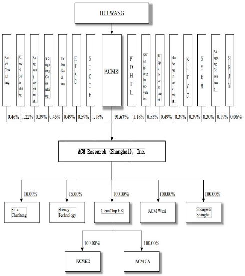
(VI) The Relationship between the Associated Shareholders and their Respective Shareholding Proportions before the Offering
Before the Offering, the association relationships between the shareholders are as follows:
| 1. | Xinshi Consulting and Xingang Consulting |
The managing partner of Xinshi Consulting and Xingang Consulting is Xindai Management Consulting (Shanghai) Co., Ltd. Xinshi Consulting and Xingang Consulting hold 0.46% and 0.19% of the Company’s shares respectively.
PDHTI holds 7.02% of SICIF’s shares. SICIF and PDHTI hold 1.18% of the Company’s shares respectively.
| | 3. | Shangrong Innovation and SRJY |
The managing partner of Shangrong Innovation and SRJY is Beijing Shang Finance Corporation. Shangrong Innovation and SRJY holds 0.53% and 0.06% of the Company’s shares respectively.
(VII) The Influence of Public Offering of Shares by the Shareholders of the Issuer on the Control, Governance Structure and Production and Operation of the Issuer
The Offering does not involve any public offering of shares by any shareholder of the Issuer.
VII. Brief Information of Directors, Supervisors, Senior Managers and Core Technicians
| (I) | Members of the Board of Directors |
The Company’s board of directors is composed of nine directors, including three independent directors. The details are as follows:
| No. | Name | Position | Nominator | Term of Office |
| 1 | HUI WANG | Chairman | ACMR | Nov.14,2019 -Nov.13,2022 |
| 2 | HAIPING DUN | Director | ACMR | Nov.14,2019 -Nov.13,2022 |
| 3 | STEPHEN SUN-HAI CHIAO | Director | ACMR | Nov.14,2019 -Nov.13,2022 |
| 4 | Charles Law | Director | ACMR | Nov.14,2019 -Nov.13,2022 |
| 5 | JIANG LI | Director | SICIF | Mar 30, 2020 -Nov.13,2020 |
| 6 | CHEN HUANG | Director | PDHTI | Mar 30, 2020 -Nov.13,2020 |
| 7 | DI ZHANG | Independent Director | Board of Directors | Nov.14,2019 -Nov.13,2022 |
| 8 | MINGXIU PENG | Independent Director | Board of Directors | Nov.14,2019 -Nov.13,2022 |
| 9 | ZHANBING REN | Independent Director | Board of Directors | Nov.14,2019 -Nov.13,2022 |
The resumes of the board members are as follows:
HUI WANG, male, born in November, 1961, an American citizen with the permanent residency in China, PH.D. of Precision Engineering, winner of Shanghai Pujiang Talent Plan. From February, 1994 to November, 1997, Mr. WANG served as the research and development manager of Quester Technology Inc. in the USA. From May, 1998 to now, Mr. WANG has served as the chairman and CEO of ACMR and the chairman of ACMSH.
HAIPING DUN, male, born in December, 1949, a Chinese Taiwan citizen with the permanent residency in USA, Ph.D. in material science and engineering. From 1983 to 2004, Mr. DUN served as a senior director in Intel Corporation. From 2008 to 2018, Mr. DUN served as the president and executive director of Champion Microelectronic Corporation. From 2003 to now, Mr. DUN has served as a director of ACMR. From May, 2005 to now, Mr. DUN has served as a director of ACMSH.
STEPHEN SUN-HAI CHIAO, male, born in April, 1948, an American citizen without the permanent residency in other countries, Ph.D. in material science and engineering. From January, 1977 to July, 1980, Stephen served as a senior scientist of Varian Medical Systems. From July, 1980 to September, 1983, Stephen served as a project manager of Hewlett Packard Enterprise Development LP. From September, 1983 to September, 1986, Stephen served as the manager of R&D Department of U.S. AMIS Company. From September, 1986 to June, 2015, Stephen served as a professor of San Jose State University. From September, 1989 to September, 2003, Stephen served as the vice president of the global enterprise development department of Mosel Vitelic Inc. From September, 1999 to now, Stephen has served as a manage director of Sycamore Management Corporation. From May, 2005 to now, Stephen has served as a director of ACMSH.
Charles Law, male, born in December, 1959, a Chinese Taiwan citizen without the permanent residency in other countries, with Master of Laws degree. From November, 1992 to January, 2001, Charles served as a managing partner of U.S. Zhongzhi Law Firm. From January, 2001 to July, 2017, Charles served as a partner of King and Wood Mallesons. From July, 2017 to now, Charles has served as a partner of U.S. Sycamore
Venture. From February, 2018 to now, Charles has served as the managing partner of Law & Law. From November, 2019 to now, Charles has served as a director of ACMSH.
JIANG LI, male, born in March, 1980, a Chinese citizen without permanent residency in a foreign country, master of management science and engineering. From September 2003 to August 2005, Mr. LI served as the sales manager of the foreign trade department of Shanghai Light Industrial International Development Corp., Ltd. From September 2005 to October 2010, Mr. LI served as the manager of the investment and development department of Shanghai Zhangjiang Medicine Public Service Platform Co., Ltd. From October 2010 to December 2016, Mr. LI served as the senior investment manager of the project investment department of Shanghai STVC (Group) Co., Ltd. From January 2017 till now, he has served as the investment director of Shanghai Integrated Circuit Industry Investment Fund Co., Ltd. From March, 2020 to now, Mr. LI has served as a director of ACMSH.
CHEN HUANG, male, born in January, 1991, a Chinese citizen without permanent residency in a foreign country, master of East Asian Development Studies, master of Business Administration, senior economist. From August 2014 to August 2015, Mr. HUANG served as the assistant of the strategic department of Shanghai Pudong Financing Guarantee Co., Ltd. From September, 2015 to October, 2016, Mr. HUANG served as the risk control manager of Shanghai Pudong Financing Guarantee Co., Ltd. From October, 2016 to January, 2020, Mr. HUANG served successively as the manager of the strategic planning and information department, the investment manager of the second investment department, and the assistant to the general manager of the second investment department of SPINNOTEC Group Co., Ltd. From February 2020 to now, Mr. HUANG has served as the assistant to the general manager of the first investment department of SPINNOTEC Group Co., Ltd. From March 2020 till now, Mr. HUANG has served as a director of ACMSH.
DI ZANG, male, born in March, 1957, a Chinese citizen without permanent residency in a foreign country, Ph.D. in material science, winner of the National Natural Science Award (Second Class Prize), and winner of “May 1 Labor Metal” in Shanghai. From 1988 to now, Mr. ZHANG has served as a teacher in Shanghai Jiaotong University. In December, 1993, Mr. ZHANG served as a professor in Shanghai Jiaotong University. Currently he serves as a chair professor in Shanghai Jiaotong University, the director of the State Key Laboratory of Metal Matrix Composites and a distinguished professor of “Cheungkong Scholars” of the Ministry of Education. From June, 2019 to now, Mr. ZHANG has served as a director of ACMSH.
MINGXIU PENG, female, born in February, 1962, a Chinese Taiwan citizen, without the permanent residency in other countries, Master of Business Administration and EMBA. From January 1999 to July 2019, she served successively as the chief financial officer, deputy general manager, chairman, CEO of Champion Microelectronic Corporation. Currently she serves as the chairman of Haiye Investment Co., Ltd. From November, 2019 to now, she has served as a director of ACMSH.
ZHANBING REN, male, born in May, 1959, a Swiss citizen with the permanent residency in China, Doctor of Engineering, an academician of Swiss Academy of Engineering Sciences. From September, 1994 to September, 1996, Mr. REN served as a production engineer in Swiss Bobst. From October, 1996 to August, 2011, Mr. REN successively held the posts of the production manager (Shanghai), general manager (Shanghai), president (Greater China) and top management member, regional operations manager (Asia), and president (Great China and Southeast Asia) in Bobst Group. From September, 2011 to December, 2013, Mr. REN served as the president (Asia Pacific) in GF Piping Systems. From January, 2014 to now, Mr. REN has served as the managing director at Shanghai SinoSwiss International Trading Co., Ltd. From July, 2015 to October, 2017, Mr. REN served as the general manager of China Banknote SICPA Security Ink Co., Ltd. From January, 2018 to now, Mr. REN has served as the managing director of Shanghai Mengtebao International Trade Co., Ltd. From November, 2019 to now, Mr. REN has served as a director of ACMSH.
(II) Members of the Supervisory Board
The Supervisory Board of the Company consists of three supervisors, among
which, one supervisor is an employee representative supervisor, specifically:
| No. | Name | Position | Nominator | Term of Office |
| 1 | TRACY DONG LIU | Supervisor | ACMR | Nov.14,2019 -Nov.13,2022 |
| 2 | QIAN DONG | Supervisor | ACMR | Mar 30, 2020 -Nov.13,2020 |
| 3 | QIAN LI | Employee Representative Supervisor | General Meeting of Employee Representative | Nov.14,2019 -Nov.13,2022 |
The resumes of the supervisory board members are as follows:
TRACY DONG LIU, female, born in November 1964, an American citizen without permanent residence of other countries. She has obtained an accounting master degree and registered as U.S. certified public accountant. She served as a Financial Controller of the San Jose Radisson Hotel in the U.S. from January 1994 to June 1995, as an Accounting Manager of KPMG from January 1996 to April 2000, as a Senior Accounting Manager of Deloitte from May 2000 to May 2005, and she has served as a Founder and Managing Partner of H&M Int’l CPAs, LLP from June 2005 to date, as a director of ACMR from September 2016 to date, and as a supervisor and president of the supervisory board of ACMSH from November 2019 to date.
QIAN DONG, female, born in March 1955, a Chinese citizen without permanent residency in a foreign country. She is a bachelor majoring in Chinese. She served as a worker of Shanghai Fengshou Tractor Factory from November 1972 to February 1979, as deputy secretary of Youth League Committee, HR head of Shanghai Light Industry School from March 1979 to March 1989, as general manager’s assistant and office director of Shanghai Dongfang Storage Tank Ltd. from April 1989 to January 1997, as secretary of board of directors and office director of Shanghai Belling Co., Ltd. from February 1997 to October 2001, as deputy general manager of business development of Premier Devices Inc. from October 2001 to February 2004, as deputy general manager and office director of Spreadtrum Communications, Inc. from March 2004 to November 2014, and she has held the post of consultant of Ruizhang Technology Co., Ltd. from November 2014 to date, and of general manager of Yunnan Energy Investment Ruizhang Internet of Things Technology Ltd. from April 2019 to date. She has served as a supervisor of ACMSH from March 2020 to date.
QIAN LI, female, born in January 1995, a Chinese citizen without permanent residency in a foreign country. She is a bachelor majoring in management. She has served as an assistant of the chairman’s office of ACMSH from July 2017 to date. She has served as a supervisor of ACMSH from November 2019 to date.
(III) Senior Managers
The Company has 5 senior managers in total, including general manager, deputy general manager, person in charge of financial matters and secretary of board of directors, etc., specifically:
| No. | Name | Position |
| 1 | JIAN WANG | General Manager |
| 2 | FUPING CHEN | Deputy General Manager |
| 3 | SOTHEARA CHEAV | Deputy General Manager |
| 4 | LISA YI LU FENG | Person in Charge of Financial Matters |
| 5 | MINGZHU LUO | Secretary of Board of Directors |
The resume of each senior manager of the Company is as follows:
JIAN WANG, male, born in February 1965, a Chinese citizen without permanent residency in a foreign country. He is a master majoring in mechanics and computer
science. He served as a technician of Hangzhou Xihu Television Factory from July 1986 to April 1987, as a technician of Japan Fuji Fine Printing Corporation from April 1996 to December 1999, as a process engineer and deputy general manager of ACMSH from December 2001 to April 2019 and as General Manager of ACMSH from May 2019 to date, and he has successfully researched and developed stress-free copper polishing and electrochemical copper plating technology, participated in and applied for more than 100 patents, and been responsible for various significant scientific research projects.
FUPING CHEN, male, born in August 1981, a Chinese citizen without permanent residency in a foreign country. He is a master majoring in materials science. He successively served as an engineer and deputy manager of SK Hynix semiconductor (China) Co., Ltd. from April 2006 to January 2010, and as a project manager, technical manager, technical director and senior director of ACMSH from January 2010 to December 2017. He has served as Deputy General Manager of ACMSH from January 2018 to date, who has participated in and successfully researched and developed advanced packaging wet processing equipment, SAPS uniwafer cleaning equipment, TEBO uniwafer cleaning equipment, Tahoe uniwafer tank combined cleaning equipment and full automatic tank cleaning equipment, he has published 5 academic papers and participated in and applied for more than one hundred patents.
SOTHEARA CHEAV, male, born in March 1952, an American citizen without permanent residency of other countries. He is a bachelor majoring in technology of electronics. He successively served as a manager of manufacturing department, director of manufacturing department from March 2007 to December 2014. He has served as deputy general manager of ACMSH from January 2015 to date.
LISA YI LU FENG, female, born in April 1958, an American citizen without permanent residency of other countries. She has obtained an accounting mater degree. She served as a regional financial director of Lumenis Inc. from January 2004 to August 2008, as financial director of Amlogic (CA) Co., Inc. from August 2008 to September 2017, as financial director of ACMR from September 2017 to November 2019, and has served as a person in charge of financial matters of ACMSH from May 2019 to date.
MINGZHU LUO, female, born in August 1983, a Chinese citizen without permanent residency in a foreign country. She is a bachelor majoring in veterinary medicine. She has successively served as assistant of president, manager of president office and director of president office of ACMSH from December 2006 to October 2019. She has served as secretary of board of directors of ACMSH from November 2019 to date.
(IV) Key Technician
The Company determines key technicians based on the following standards: (1) responsible persons or core members of the Company and departments in connection with research and development; (2) relevant persons responsible for the direction of research and development and processing improvements which are significant to the business development and future development strategy of the Company; (3) relevant persons who have contributed to intellectual property rights and core technologies of the Company. The Company has 6 key technicians in total, specifically:
| No. | Name | Position |
| 1 | HUI WANG | Chairman |
| 2 | JIAN WANG | General Manager |
| 3 | FUPING CHEN | Deputy General Manager |
| 4 | SOTHEARA CHEAV | Deputy General Manager |
| 5 | JUN WANG | Vice President of Electrical Engineering |
| 6 | XUEJUN LI | Vice President of After-sale Services |
The resume of each key technician of the Company is as follows:
HUI WANG, please refer to “VII (I) Members of Board of Directors” in this Section for his resume.
JIAN WANG, please refer to “VII (III) Senior Managers” in this Section for his resume.
SOTHEARA CHEAV, please refer to “VII (III) Senior Managers” in this Section for his resume.
FUPING CHEN, please refer to “VII (III) Senior Managers” in this Section for his resume.
JUN WANG, male, born in March 1984, a Chinese citizen without permanent residency in a foreign country. He is a master majoring in electronics and communication engineering. He successively served as an electrical engineering manager, senior manager and director of electrical engineering of ACMSH from May 2007 to April 2020, and has served as vice president of electrical engineering of ACMSH from May 2020 to date, being responsible for the design of all equipment and electrical control system and team building. He has participated in relevant patent applications of TEBO uniwafer cleaning equipment and Tahoe uniwafer tank combined cleaning equipment and been responsible for Chinese 02 Technology Significant Special Research and Development Projects-“Research and Development of 65-45nm Copper Interconnection Stress-free Polishing Equipment” and “Reseach, Development and Application of 20-14nm Copper Interconnection Copper Plating Equipment”, and the development of electronical control system of the project of “Research, Development and Industrialization of Uniwafer Tank Combined Cleaning Equipment” which is a Significant Project of Shanghai Strategic Emerging Industry.
XUEJUN LI, male, born in May 1970, being a Chinese citizen without permanent residency in a foreign country. He is a bachelor majoring in electric automatization. He successively served as a manager of after-sale services, senior manager, director of after-sale services from May 2009 to April 2020. He has served as vice president of after-sale services of ACMSH from May 2020 to date, being responsible for the provision of technical services to clients and the construction of after-sale service team. He has participated in the research and development and patent applications of technologies in connection with semiconductor cleaning equipment, provided product technical supports and solutions to main clients of the Company, and focused on the improvement of production efficiency and product yield of clients.
(V) Information on Positions in other Companies held by Directors, Supervisors, Senior Managers and Key technicians of the Company
As of the date of signing the [***], positions in other companies held by the directors, supervisors, senior managers and key technicians of the Company are as follows:
| Name | Position in the Company | Name of Employer | Position | Relationship with the Issuer |
HUI WANG | Chairman | ACMR | Chairman, CEO | Controlling Shareholder |
| ACM Research(Cayman) | Director | Related party |
| NINEBELL | Director | Related party |
| HAIPING DUN | Director | ACMR | Director | Controlling Shareholder |
| STEPHEN SUN-HAI CHIAO | Director | Sycamore Management Corporation | Managing Partner | Related party |
| Silicon Technology Investment (Cayman) Corp. | Director | Related party |
| Charles Law | Director | Law and Law | Managing Partner | Related party |
|
| Sycamore Management Corporation | Partner | Related party |
| Nanjing Shuige Investment and Management Consultancy Co., Ltd. | Supervisor | None |
| CHEN HUANG | Director | Shanghai Pudong Technology Innovation Group Co., Ltd. | Investment I Department Assistant General Manager | None |
| ASR Microelectronics (Shanghai) Co., Ltd. | Director | Related party |
| Ideal Energy (Shanghai) Sunflower Thin Film Equipment Ltd. | Director | Related party |
| JIANG LI | Director | Shanghai Integrated Circuit Industry Investment Fund Management Co., Ltd. | Investment Director | None |
| SMIC Southern Integrated Circuit Manufacturing Co., Ltd. | Supervisor | None |
| Shanghai Jita Semiconductor Co, Ltd. | Director | Related party |
| EverDisplay Optronics (Shanghai) Limited | Director | Related party |
| Shanghai Qiyuji Sports Technology Development Co., Ltd. | Supervisor | None |
| DI ZHANG | Independent Director | School of Materials Science and Engineering, Shanghai Jiao Tong University | Professor | None |
| MINGXIU PENG | Independent Director | Haihua Investment Co., Ltd. | Chairman | None |
| Avision Inc. | Independent Director | None |
| Qifa Electronics Co., Ltd. | Director | None |
| Longcai Technology Co., Ltd. | Director | None |
| Mars Semiconductor Corp. | Independent Director | None |
| ZHANBING REN | Independent Director | Shanghai Mengtebao International Trading Co., Ltd. | Executive Director | None |
| Shanghai Ruizhong International Trading Co., Ltd. | Executive Director | None |
| Black Peony (Group) Co., Ltd. | Independent Director | None |
| TRACY DONG LIU | Supervisor | ACMR | Director | Controlling Shareholder |
| H&M Int’l CPAs, LLP | Managing Partner | Related party |
| QIAN DONG | Supervisor | Yunnan Energy Investment Ruizhang Internet of Things Technology Ltd. | Director and General Manager | Related party |
| | | Shanghai Viewnoon Information
Technology Co., Ltd. | Director | Related party |
| | | Shanghai Zhaonengkun Information | Director | Related party |
|
| Technology Co., Ltd. |
|
|
| Shanghai Zhimeng Internet of Things Technology Co., Ltd. | Executive Director and General Manager | Related party |
| JIAN WANG | General Manager | ShengYuan Management Consulting (Shanghai) Co., Ltd. | Executive Director | Related party |
| FUPING CHEN | Deputy General Manager | Wuxi Hengchuang Micro-Technology Ltd. | Supervisor | None |
| MINGZHU LUO | Secretary of Board of Directors | ShengYuan Management Consulting (Shanghai) Co., Ltd. | Supervisor | Related party |
| Shengyi Technology | Director | Shareholding Subsidiary |
(VI) Family Relation among Directors, Supervisors, Senior Managers and Key technicians of the Company
As of the date of signing the [***], except for the brotherhood relation between the Chairman, HUI WANG, and the General Manager, JIAN WANG, there is no family relation among directors, supervisors, senior managers and key technicians of the Company.
VIII. Agreements between the Company and any of Directors, Supervisors, Senior Managers and Key technicians and their Performance
As of the date of signing the [***], the Company has entered into the Labor Contract, the Non-competition Agreement and the Confidentiality and Intellectual Property Protection Agreement regarding horizontal competition and confidentiality matters with each director, supervisor, senior manager and key technician who works in and receives remuneration from the Company, and the Company and directors, supervisors, senior managers and key technicians are protected and bound by provisions of relevant labor contracts.
The first Extraordinary General Meeting of the Company in 2019 resolved to pass the Proposal on 2019 Stock Option Incentive Plan (Draft) of the Company on November 29, 2019, pursuant to which, the Company entered into the Stock Option Grant Agreement with its directors, senior managers, key technicians, key employees, etc.
Except for the above, none of director, supervisor, senior manager and key technician of the Company enters into any other contract or agreement with the Company. As of the date of signing the [***], the above contracts or agreements are performed normally without any default.
IX. Changes in Directors, Supervisors, Senior Managers and Key technicians of the Company within the Last Two Years
(I) Changes in Directors of the Company
The board of directors of ACMSH consisted of HUI WANG, HAIPING DUN, STEPHEN SUN-HAI CHIAO early 2018.
The board of directors of ACMSH resolved that Charles Law and DI ZHANG
were elected as additional members of the board of directors of the Company on June 26, 2019.
The establishment meeting and the first general meeting of shareholders of the Company elected HUI WANG, HAIPING DUN, STEPHEN SUN-HAI CHIAO, Charles Law, DI ZHANG, MINGXIU PENG and ZHANBING REN as members of the first-session board of directors of the Company on November 14, 2019.
The first Extraordinary General Meeting of the Company in 2020 elected CHEN HUANG, JIANG LI as members of the first-session board of directors of the Company on March 30, 2020.
In the last two years, the reasons for changes in directors of the Company are the nomination of newly elected directors after changes in shareholders of the Company and the establishment of independent director system after the Company is changed into a joint stock company in its entirety.
(II) Changes in Supervisors of the Company
The supervisor of ACMSH was TRACY DONG LIU early 2018.
The establishment meeting and the first general meeting of shareholders of the Company elected TRACY DONG LIU and SHOULEI JIANG as members of the supervisory board of the Company, and the first-session supervisory board of the Company comprised the above two supervisors and QIAN LI, the employee representative supervisor elected by the general meeting of employees of the Company, on November 14, 2019.
SHOULEI JIANG, a supervisor of the Company, resigned as supervisor for personal reasons and the first extraordinary general meeting of shareholders of the Company in 2020 elected QIAN DONG as a member of the first-session supervisory board.
In the last two years, the main reasons for changes in supervisors of the Company are the nomination of newly elected supervisors after changes in shareholders of the Company and further perfection of the governance structure of the Company and election of employee supervisor after the Company became a joint stock company.
(III) Changes in Senior Managers
The senior managers of the Company comprised HUI WANG. The board of directors of ACMSH resolved to pass the appointment of JIAN WANG as the general manager of the Company and LISA YI LU FENG as the person in charge of financial matters in May 2019.
In November 2019, the first meeting of the first-session board of directors of ACMSH resolved to approve the appointment of JIAN WANG as the general manager of the Company, FUPING CHEN and SOTHEARA CHEAV as deputy general managers, LISA YI LU FENG as the person in charge of financial matters and MINGZHU LUO as the secretary of board of directors.
In the last two years, HUI WANG, a senior manger of the Company, no longer held his position for personal reasons, and other senior managers were engaged by the board of directors after the Company was changed into a joint stock company in its entirety. All of the above persons hold positions in the Company during the Reporting Period, and there is no material change in senior managers of the Company.
(IV) Changes in Key Technicians
In the last two years, there is no change in key technicians of the Company.
X. External Investments Made by Directors, Supervisors, Senior Managers and Key Technicians of the Company
As of the date of signing the [***], external investments made by directors, supervisors, senior managers and key technicians of the Company are as follows:
| Name | Position in the Company | Name of Investee | Shareholding Percentage | Relationship with the Issuer |
| STEPHEN SUN-HAI CHIAO | Director | Green Expedition LLC | 100% | Related party |
| ZHANBING REN | Independent Director | Shanghai Mengtebao International Trading Co., Ltd. | 50% | Related party |
| Shanghai Ruizhong International Trading Co., Ltd. | 30% | Related party |
| QIAN DONG | Supervisor | Shanghai Zhimeng Internet of Things Technology Co., Ltd. | 60% | None |
| Shanghai Lianwan Investment Management Center (Limited Partnership) | 50% | Related party |
| Shanghai Zhaonengkun Information Technology Co., Ltd. | 12.14% | None |
| Xinwei Consulting | 3.23% | Shareholder |
| JIAN WANG | General Manager | ShengYuan Management Consulting (Shanghai) Co., Ltd. | 100% | Related party |
| FUPING CHEN | Deputy General Manager | Shengxin Shanghai | 2.94% | Related party |
| MINGZHU | Secretary of Board of
| 1.55% | |
XI. Shares Held by Directors, Supervisors, Senior Managers and Key technicians of the Company and their Immediate Relatives
As of the date of signing the [***], none of director, supervisor, senior manager and key technician of the Company and their immediate relatives directly hold any share of the Company, information on shares of the Company indirectly held by the above persons is as follows:
Company holding the shares of the Company | Relationship with the Issuer | Name | Position/Family Relation | Information on Shareholding |
| ACMR | Holding 91.67% of shares in the Company | HUI WANG | Chairman | Holding 168,006 Class A shares and 1,146,934 Class B shares of ACMR, indirectly holding 206,667 Class A shares and 60,000 Class A shares of ACMR through David Hui Wang & Jing Chen Family Living Trust and David Hui Wang & Jing Chen Irrevocable Trust respectively, and indirectly holding 7,334 Class B shares of ACMR through David Hui Wang & Jing Chen Irrevocable Trust |
| JING CHEN | Spouse of HUI
| Holding 33,334 Class B shares of ACMR, indirectly holding 206,667
|
| | | | WANG | Class A shares and 60,000 Class A shares of ACMR through David Hui Wang & Jing Chen Family Living Trust and David Hui Wang & Jing Chen Irrevocable Trust respectively, and indirectly holding 7,334 Class B shares of ACMR through David Hui Wang & Jing Chen Irrevocable Trust |
| | | BRIAN WANG | Son of HUI WANG | Holding 117,334 Class B shares of ACMR |
| | | SOPHIA WANG | Daughter of HUI WANG | Holding 15,279 Class A shares and 117,334 Class B shares of ACMR |
| | | HAIPING DUN | Director | Hoding 285,030 Class A shares and 100,000 Class B shares of ACMR |
| | | STEPHEN SUN-HAI CHIAO | Director | Holding 69,815 Class B shares of ACMR, indirectly holding 55,000 Class A shares of ACMR through Green Expedition LLC, and indirectly holding 30,000 Class B shares of ACMR through Stephen Sun-Hai And Mary Wu-Chun Chiao Revocable Trust |
| | | Charles Law | Director | Holding 30,112 Class A shares of ACMR |
| | | ZHANBING REN | Independent Director | Holding 3,334 Class B shares of ACMR |
| | | TRACY DONG LIU | Supervisor | Holding 16,924 Class A shares of ACMR |
| | | JIAN WANG | Deputy General Manager | Holding 84,386 Class A shares and 50,001 Class B shares of ACMR |
| | | SOTHEARA CHEAV | Deputy General Manager | Holding 43,334 Class A shares of ACMR |
| | | LISA YI LU FENG | Person in Charge of Financial Matters | Holding 6,943 Class A shares of ACMR |
| | | XUEJUN LI | Key Technician | Holding 800 Class A shares of ACMR |
| Xinwei Consulting | Holding 1.22% of shares in the Company | QIAN DONG | Supervisor | Holding 3.23% of shares in Xinwei Consulting |
| Xinshi Consulting | Holding 0.46% of shares in the Company | JUN WANG | Key Technician | Holding 5.40% of shares in Xinshi Consulting |
| XUEJUN LI | Key Technician | Holding 5.40% of shares in Xinshi Consulting |
Note: The data on the percentage of shares held by the above persons in ACMR is as of December 31, 2019.
XII. Information on Remuneration of Directors, Supervisors, Senior Managers and Key Technicians of the Company
(I) Composition, Basis of Determination, Procedures Performed of Remuneration and its Percentage
The remuneration of directors, supervisors, senior managers and key technicians who hold positions responsible for specific business in the Company consists of basic salary, year-end bonus, etc. Based on the needs of each position, duties and working performance, the Company will pay equitable and reasonable salary in accordance with remuneration regulations and ensure that all of remuneration and benefits of employees are competitive in the same industry and market. The Compensation and Appraisal Committee of the Company formulates remuneration policies and plans of directors and senior managers, conducts appraisals on performance of duties of directors and senior managers and submits the results to the board of directors or the general meeting of shareholders for review and deliberation; independent directors of the Company receive fixed allowances.
During the Reporting Period, the total remuneration for directors, supervisors, senior managers and key technicians of the Company are RMB 3,178,800 Yuan, RMB 4,467,700 Yuan and RMB 5,780,600 Yuan respectively, accounting for 23.83%, 4.34% and 3.76% of total profit of the Company for each period.
(II) Remuneration Received by Directors, Supervisors, Senior Managers and Key technicians from the Issuer in the Latest Year
Information on remuneration received by directors, supervisors, senior managers and key technicians from the Company in 2019 is as follows:
Unit: RMB 10,000 Yuan
| No. | Name | Position | Remuneration in 2019 |
| 1 | HUI WANG | Chairman | 61.87 |
| 2 | HAIPING DUN | Director | - |
| 3 | STEPHEN SUN-HAI CHIAO | Director | - |
| 4 | Charles Law | Director | - |
| 5 | CHEN HUANG | Director | - |
| 6 | JIANG LI | Director | - |
| 7 | DI ZHANG | Independent Director | 5.14 |
| 8 | MINGXIU PENG | Independent Director | 1.30 |
| 9 | ZHANBING REN | Independent Director | 1.30 |
| 10 | TRACY DONG LIU | Supervisor | 0.78 |
| 11 | QIAN DONG | Supervisor | - |
| 12 | QIAN LI | Employee Representative Supervisor | 9.18 |
| 13 | JIAN WANG | General Manager | 65.81 |
| 14 | FUPING CHEN | Deputy General Manager | 74.74 |
| 15 | SOTHEARA CHEAV | Deputy General Manager | 76.58 |
| 16 | LISA YI LU FENG | Person in Charge of Financial Matters | 98.81 |
| 17 | MINGZHU LUO | Secretary of Board of Directors | 41.56 |
| 18 | JUN WANG | Key Technician | 74.83 |
| 19 | XUEJUN LI | Key Technician | 65.38 |
Note: 1. Certain directors of the Company do not receive any remuneration from the Company; 2. The allowance of each independent director of the Company is RMB 100,000 Yuan/year; 3. QIAN DONG served as supervisor in March 2020, and did not receive any remuneration in 2019.
(III) Other Treatments and Pension Plans for the Above Persons of the Company
As of the date of signing the [***], the Company has not formulated any other treatments, pension plans, etc.for its directors, supervisors, senior managers and key technicians.
XIII. Equity Incentives and Relevant Arrangements of the Issuer prior to this Offering
(I) Employee Shareholding Platform
As of the date of signing the [***], the Issuer has established two employee shareholding platforms prior to the submission and application of this Offering: Xinshi Consulting and Xingang Consulting, each of which holds 0.46% and 0.19% of shares of the Company respectively.
| | 1. | Basic Information on Employee Shareholding Platforms |
(1) For basic information on Xinshi Consulting, please refer to “(5) Xinshi Consulting” of “VI(V) New Shareholders of the Issuer in the Latest Year” of this Section.
(2) For basic information on Xingang Consulting, please refer to “(7) Xingang Consulting” of “VI(V) New Shareholders of the Issuer in the Latest Year” of this Section.
| | 2. | Employee Shareholding Platforms’ Confirmation of Share-based Payment |
The above employee shareholding platforms become shareholders of the Company by the means of increase in capital, the price at which the capital is increased is lower than the price in the same comparable transaction, and the Company has confirmed costs of share-based payment. For specific information on the increase in capital, please refer to “(4) the Fourth Increase in Capital of ACMSH in May 2019” of “II (III) Information on the Changes of Shareholders of the Issuer”.
| | 3. | Operation of Employee Shareholding Platforms Not Subject to the “Closed Loop Principle” |
Pursuant to the partnership agreement of employee shareholding platforms, all or part of property shares in a partnership may be transferred among limited partners, and also may be transferred to a person other than partners. Therefore, such transfer has not been limited to internal transfer among specific employees only by shareholding platforms, operation of which does not conform to the “closed loop principle”.
| | 4. | Employee Shareholding Platforms Not Being Private Investment Funds |
The above employee shareholding platforms have never raised funds from investors and formed in a non-public manner, and thus are not private investment funds under the Interim Measures on the Supervision and Administration of Private Investment Funds, there is no need to go through private investment fund filings in accordance with the Measures on the Registration of Private Investment Fund Managers and Filing of Funds (Trial) or other provisions.
| | 5. | Share Lock-up Commitments of Employee Shareholding Platforms |
Each of the above employee shareholding platforms undertakes that:
(1) During 12 months as of the date on which stocks of the Issuer are listed, it will not transfer shares which are held by this enterprise and have been issued by the Issuer prior to this Offering and listing (hereinafter referred to as the “Pre-initial Offering Shares”), entrust others to manage such shares, or propose to repurchase such part of shares by the Issuer.
(2) If this enterprise decreases the Pre-initial Offering Shares held by it after the lock-up period expires, it will strictly comply with laws, administrative regulations, departmental rules, normative documents and relevant provisions of the Shanghai Stock Exchange and perform corresponding obligations of information disclosure.
(3) If this enterprise decreases its shares of the Issuer in violation of the above commitments, then actual proceeds (if any) received from the sale of such part of shares of the Issuer shall belong to the Issuer, and all losses and legal consequences resulting therefrom shall be borne by this enterprise.
(II) Option Incentive Plan Made by the Issuer for Employees
The Issuer has an option incentive plan which is formulated prior to the application of initial public offering and will be implemented after it is listed (hereinafter referred to as the “Incentive Plan”), the specific information of the plan is as follows:
| | 1. | Procedures of Formulating the Incentive Plan |
On November 14, 2019, the Company held the first session meeting of the first board of directors and resolved to pass the Proposal on the Stock Option Incentive Plan of the Company in 2019 (Draft), the Proposal on Measures on Implementing Appraisal and Administration of the Stock Option Incentive Plan of the Company in 2019, the Proposal on the Submission and Application to the General Meeting of Shareholders for Authorizing the Board of Directors to Deal With Matters in connection with 2019 Stock Option Incentive and other proposals. Independent directors issued their independent opinions consenting to the above proposals.
On November 14, 2019, the Company held the first session meeting of the first supervisory board and resolved to pass the Proposal on the Stock Option Incentive Plan of the Company in 2019 (Draft), the Proposal on Measures on Implementing Appraisal and Administration of the Stock Option Incentive Plan of the Company in 2019 and other proposals.
On November 15, 2019, the Issuer published name and position of each incentive
object in the Company internally through on-site posting in the Company and other means, the period of publicity shall not less than 10 days.
On November 25, 2019, the Company held the second session meeting of the first supervisory board and resolved to pass the Proposal on the Supervisory Board’s Explanation on Reviewing Opinions and Publicity of the List of Stock Option Incentive Objects.
On November 29, 2019, the Company held the first-session extraordinary meeting of shareholders in 2019 and resolved to pass the Proposal on the Stock Option Incentive Plan of the Company in 2019 (Draft), the Proposal on Measures on Implementing Appraisal and Administration of the Stock Option Incentive Plan of the Company in 2019, the Proposal on the Authorization to the Board of Directors to Deal With Matters in connection with 2019 Stock Option Incentive and other proposals
The Compensation and Appraisal Committee of the board of directors of the Company held the first-session extraordinary meeting in 2019 and resolved to pass the Proposal on the Adjustment of Incentive Objects and Granting Amounts of Stock Option Incentive Plan, the Proposal on Granting Stock Options to Incentive Objects and other documents, and submitted to the board of directors of the Company for review and deliberation on December 20, 2019.
On December 31, 2019, the Company held the second session meeting of the first board of directors and the third session meeting of the first supervisory board respectively, and resolved to pass the Proposal on the Adjustment of Incentive Objects and Granting Amounts of Stock Option Incentive Plan, the Proposal on Granting Stock Options to Incentive Objects and other proposals. Independent directors issued their independent opinions consenting to the above proposals.
In conclusion, the formulation of this incentive plan by the Issuer has performed necessary procedures.
| | 2. | Basic Content of the Incentive Plan |
The basic content of this incentive plan is as follows:
(1) Incentive Objects
The number of incentive objects involved in this incentive plan is 88 in total, including directors, senior managers of the Company and middle-level management personnel and core business employees of the Company and its controlled subsidiaries. The above incentive objects shall not include any independent directors or supervisors of the Company. The directors and senior managers of the Company must be elected by the general meeting of shareholders of the Company or engaged by the board of directors of the Company. Each incentive object must enter into a labor contract or engagement contract with the Company or any of controlled subsidiaries of the Company within the appraisal period of this incentive plan.
Accordingly, incentive objects under the incentive plan do not exist any circumstance as described in paragraph 2 of Article 8 of the Measures on the Administration of Equity Incentives of Listed Companies, and comply with provisions of Article 10.4 of the Rules Governing the Listing of Stocks on the STAR Market of Shanghai Stock Exchange.
(2) Relevant Clauses of the Incentive Plan
Article 1 of Chapter III of the Incentive Plan provides that “This Plan adopts stock options as tools of equity incentive. The source of stocks under this Plan shall be stocks issued by the Company specifically to incentive objects. Subject to conditions as provided for under this Plan, each stock option granted to an incentive object shall have the right to purchase one ordinary share from ACMSH at the exercise price within the exercisable period. None of stock options granted to incentive objects may be transferred or used for creating any security or repaying any debt.”
Chapter IV of the Incentive Plan provides for effective period, date of grant, waiting period and exercise arrangement of stock options, among which, Article 4 of Chapter IV provides that “The stock options will be exercised in two installments upon the expiration of 36 months after such options are granted, the exercisable options in each instalment shall account for 1/2 and 1/2 of the total amount of granted stock options respectively. Within exercisable days, subject to the fulfillment of conditions of exercise as stipulated under this Plan, each inventive object may exercise his/her stock options which have been granted to him/her in two installments in accordance with arrangements as stipulated in the table below. The period of exercise for exercisable options shall be 12 months, the beginning date of the next period of exercise shall not be earlier than the expiration date of the last period of exercise, and relevant interests shall not be deferred to the next period when conditions of exercise for stock options in each installment fail to be fulfilled.”
Chapter IX of the Incentive Plan provides for how to deal with special circumstances of the incentive plan and specifies circumstances under which the Company repurchases options or incentive objects terminate their exercise of options.
Chapter XII of the Incentive Plan provides for the formulation of this incentive plan, granting and exercising of options and other aspects.
In conclusion, the definitions of incentive tools, restrictions of rights, exercise arrangements, repurchasing or terminating exercise of options, procedures of implementation and other content involved in the incentive plan are formulated by reference to relevant provisions of the Measures on the Administration of Equity Incentives of Listed Companies.
(3) Exercise Price
The exercise price of this incentive plan is determined on the basis of the transaction price in the most recent increase in capital of ACMSH by investors, and thus the exercise price shall be RMB 13 Yuan per share.
The price per share shall be RMB 0.66 Yuan on the basis of the audited net assets of ACMSH in the most recent one year, and the price per share shall be RMB 3.52 Yuan on the basis of the value as estimated in the most recent period. Accordingly, this
incentive plan is not less than the audited net assets or estimated value in the most recent year.
(4) Total Amount of Granted Stock Options
The first Extraordinary General Meeting of the Issuer in 2019 reviewed and passed the 2019 Option Incentive Plan and the 2019 Appraisal Administration Measures and agreed to grant 5,677,500 stock options, representing 1.46% of the total amount of capital shares of the Company as of such grant, to 88 qualified incentive objects after adjustment. The effective period shall not exceed 72 months from the date on which stock options are granted to the date on which all stock options granted to incentive objects are exercised or cancelled.
Accordingly, the percentage of shares in connection with all of the Issuer’s option incentive plans which are within effective period to the total amount of capital shares of the Company immediately prior to the listing of the Company does not exceed 15%, and none of reserved interests is created.
(5) Waiting Period
The waiting period shall be 36 months as of the date on which stock options are granted. Within the waiting period, none of incentive objects shall exercise any of options which are granted in accordance with this plan.
(6) No Change in de facto controller will be Caused
According to the total amount of stock options granted under this incentive plan, the de facto controller of the Company will not be changed resulting from any exercise of options of the Issuer after the listing.
(7) Lock-up Commitments
According to Article 4 of Chapter IV of the Incentive Plan, if the time point of exercising stock options under this incentive plan is after the listing of the Company, then: (i) none of incentive objects shall decrease his/her stocks acquired resulting from his/her exercise of options after the Company is listed within 3 years; (ii) upon the expiration of the above lock-up period, each incentive object shall decrease his/her stocks by reference to relevant provisions of decreasing stocks by directors, supervisors and senior managers of the Company, and comply with then relevant laws, regulations, normative documents and rules of the stock exchange where the Company is listed.
| | 3. | Effects of the Equity Incentives on the Company |
Through the formulation of this incentive plan, the Company is intended to motivate working enthusiasm of managers, key technicians, key employees of the Company, realize the unification of objectives of shareholders, the Company and employees and promote the operating efficiency of the Company.
After any grant is made under this incentive plan, the costs of share-based payment confirmed due to amortization of cost incurred by stock options will be increased, which will cause certain effect on the operational performance of the Company in the future.
Under the equity incentive plan of the Company, each incentive object who has received equity options will hold no more than 1% of stocks in the Company after his/her exercise, which will not cause any significant effect on the shareholding structure of the Company, and the equity incentives will not affect the controlling power over the Company.
| | 4. | Accounting Treatments of Equity Incentives |
According to relevant provisions on the determination of fair value in the Accounting Standards for Business Enterprises No.11-Share-based Payment and the Accounting Standards for Business Enterprises No.22-Determination and Measurement of Financial Tools issued by the Ministry of Finance, it is necessary to select an appropriate valuation model to calculate the fair value of stock options. The cost of stock options granted under this incentive plan is estimated based on the Black-Scholes model.
The cost of stock options granted under this incentive plan shall be amortized before each instalment of options becomes exercisable, and the actual accounting cost shall be revalued based on such parameters as actual stock prices and volatility on the date of grant as determined by the board of directors. Therefore, the amortization of the cost of stock options will cause certain effect on the operational performance of the Company.
During the Reporting Period, the Company does not involve any share-based payment resulting from this incentive plan which will cause effect on the operational performance of the Company.
| | 5. | Verification Opinions of Intermediary Agencies |
Upon verification, the Sponsor and the Reporting Accountant consider that:
(1) The formulation and implementation of the above option incentive plan have performed necessary decision-making procedures, and incentive objects comply with provisions of Article 10.4 of the Rules Governing the Listing of Stocks on the STAR Market of Shanghai Stock Exchange;
(2) The Issuer has fully disclosed relevant information of the option incentive plan in the [***];
(3) The measurement methods and results of fair value with respect to equity instruments in connection with share-based payment of the Issuer is reasonable;
(4) Relevant accounting treatments with respect to share-based payment of the Issuer comply with relevant provisions of the Accounting Standards for Business Enterprises.
(III) Stock Options Acquired by Employees of the Issuer in the Controlling Shareholder of the Issuer
Since the establishment of ACMR, the controlling shareholder of the Company, has granted stock options of ACMR to certain employees in order to establish and perfect long-acting incentive mechanism, maintain stability of core team and fully motivate enthusiasm of core and key employees of the Company. As of December 31, 2019, HUI WANG, the de facto controller of the Company, held 1,053,335 stock options of ACMR, and other employees of the Company held 1,702,513 stock options of ACMR in total.
During the Reporting Period, the Company has confirmed costs of share-based payment for stock options of ACMR acquired by the above persons, the amount of which is RMB 1.7247 million Yuan, RMB 3.9978 million Yuan and RMB 7.3990 million Yuan respectively.
XIV. Employees of the Issuer and their Social Securities
(I) Employees
As at the end of each Reporting Period, the number of employees of the Company is 187, 270 and 358 respectively. As of December 31, 2019, the professional structure, educational level and age distribution of employees of the Company are as follows:
| Professional Structure of Employees | | Percentage of Total Number of Employees |
| Management Personnel | 29 | 8.10% |
| Marketing Sales Personnel | 10 | 2.79% |
| After-sales Service Personnel | 76 | 21.23% |
| Production Personnel | 84 | 23.46% |
| Finance Personnel | 9 | 2.51% |
| Technology Research and Development Personnel | 150 | 41.90% |
| Total | 358 | 100.00% |
| Educational Level of Employees | Headcount | Percentage of Total Number of Employees |
| Master degree and above | 72 | 20.11% |
| Bachelor degree | 140 | 39.11% |
| College degree and below | 146 | 40.78% |
| Total | 358 | 100.00% |
| Age Distribution of Employees | Headcount | Percentage of Total Number of Employees |
| 50 and above | 13 | 3.63% |
| 40-49 | 28 | 7.82% |
| 30-39 | 162 | 45.25% |
| 30 and below | 155 | 43.30% |
| Total | 358 | 100.00% |
(II) Implementation of Social Security System by the Issuer
The Company and its domestic subsidiaries implement the system of labor contract, they enter into a labor contract with each employee in accordance with the Labor Law. The Company and its domestic subsidiaries have bought social insurances, such as pension insurance, medical insurance, unemployment insurance, employment injury insurance and maternity insurance, and contributed housing provident funds for their employees in accordance with national and local laws and regulations in connection with social security.
Each foreign subsidiary of the Company has entered into a labor contract with each foreign employee and implemented the system of social security in accordance with laws and regulations of the place where the subsidiary is located.
During the Reporting Period, there is no dispute or litigation of the Issuer and its subsidiaries arising out of the issue of payment of social insurance, nor is there any administrative punishment arising out of the issue of payment of social insurance premiums. As of the execution date of this [***], all of the number of employees, base number, percentage, etc. of social insurance premiums paid by the Issuer for employees comply with provisions of laws, regulations and normative documents. The Issuer has contributed housing provident funds for Chinese employees of the Company in accordance with provisions of national and local governmental authorities.
According to the reply letter issued by Huangpu Sub-center of Shanghai Social Security Business Administration Center on May 20, 2020, ACMSH has no overdue premium of social securities during the period from January 1, 2017 to December 31, 2019.
According to the certificate issed by Xinwu District Human Resources and Social Security Bureau of Wuxi on April 24, 2020, it is not found that ACM Wuxi has any violation of laws, regulations or rules in connection with labor security or any adverse record that ACM Wuxi is subject to any administrative penalty or administrative process imposed by labor administration departments due to its violation of laws during the period from January 1, 2017 to April 13, 2020.
According to the certificate issued by Shanghai Housing Provident Fund Administration Center on March 10, 2020, ACMSH has established a housing provident fund account, and the housing provident fund account is in the status of normal contribution without any administrative punishment record imposed by the Housing Provident Fund Administration Center.
According to the certificate issued by Wuxi Housing Provident Fund Administration Center on April 13, 2020, during the period commencing from January 1, 2017 to the date of issuance of the certificate, ACM Wuxi has never been subject to any recovery for its failure of contribution, fine or any other form of administrative punishment imposed by Wuxi Housing Provident Fund Administration Center arising out of any of its violation of housing provident fund regulations.
Section VI Business and Technology
Ⅰ. Main Business and Main Products of the Issuer
(Ⅰ) Main business, main products and income component
| | 1. | Basic situation of main business |
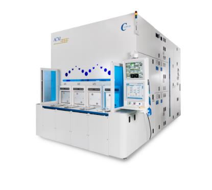
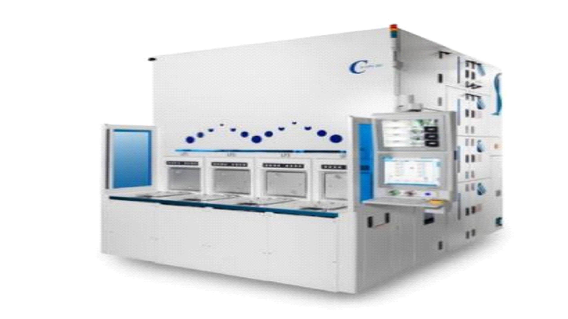
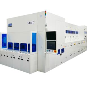
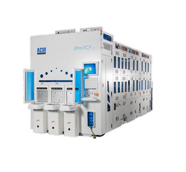
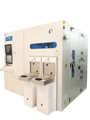
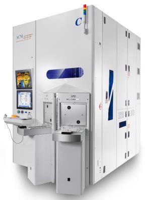
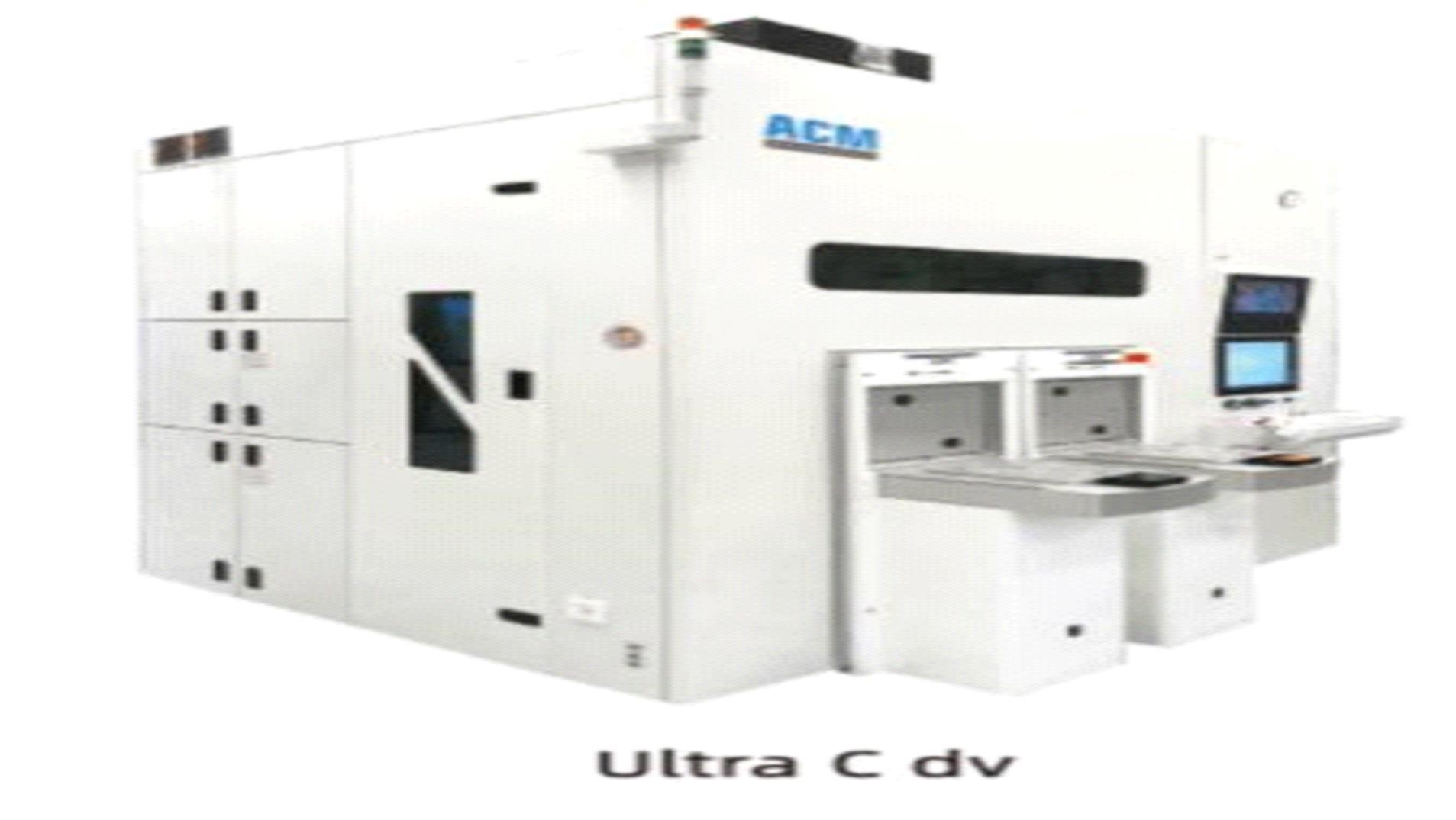
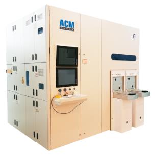
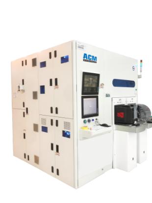
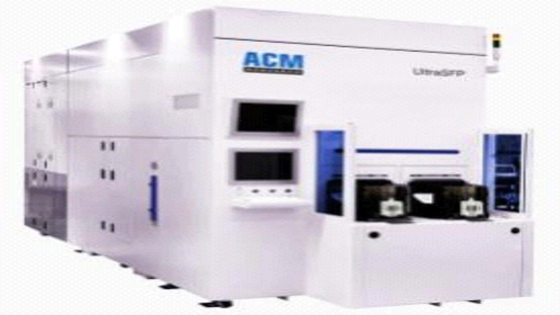
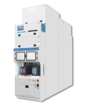
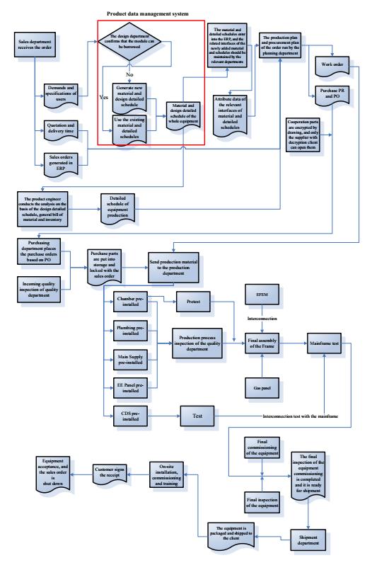
The company is mainly occupied in the research, development, production and sales of semiconductor special equipment. Its main products include semiconductor cleaning equipment, semiconductor electroplating equipment and advanced packaging wet equipment. The company persists in the development strategy of differentiated competition and innovation. Through self-developed single-chip megasonic cleaning technology, single-chip slot-type combined cleaning technology, electroplating technology, stress-free polishing technology and vertical furnace tube technology, the company provides customized equipment and process solutions to global wafer manufacturing, advanced packaging and other customers, effectively improving the customer’s production efficiency, product yield and reduce production costs.
Based on independent innovation, the company has successfully developed the world’s first SAPS and TEBO megasonic cleaning technology and Tahoe single-chip slot-type combined cleaning technology through years of technological research and process accumulation. These technologies can be applied in the wafer cleaning field of 45nm and below technology nodes, which can effectively solve the cleaning problem of organic contamination and particle after etching, and significantly reduce the use of concentrated sulfuric acid and other chemical reagents. It helps customers reduce production costs while meeting the energy saving and emission reduction requirements.
With advanced technology and rich product lines, the company has developed into one of the few semiconductor special equipment providers with certain international competitiveness in Chinese Mainland. The company’s products have been recognized by many mainstream semiconductor manufacturers at home and abroad, and have obtained good market reputation. The main customers of the company are as follows:
| Number | Field of Customer | Name of Customer |
| 1 | Wafer manufacturing | Hynix, Huahong Group, Yangtze Memory, SMIC, Hefei Changxin |
| 2 | Advanced Packaging | JCET, TFME, SJsemi, Nepes |
| 3 | Manufacturing and recycling of semiconductor silicon wafer | ZING SEMI, Wafer Works, Wafer Works, PSI |
| 4 | Research institutes | Institute of Microelectronics of Chinese Academy of Sciences, Shanghai Integrated Circuit, NCAP |
The company’s technical level for the megasonic single-chip cleaning equipment, single-chip slot-type combined cleaning equipment and electroplating process equipment of copper interconnection, has reached international leading or international advanced level. As of December 31, 2019, the company and its holding subsidiaries has 232 main licensed patents, including 108 domestic patents and 124 overseas patents. Among them, there are 227 invention patents. The company also won the title of “Shanghai Key Laboratory of Advanced Wet Process Equipment for Integrated Circuits”. It is the main subject unit of major scientific research projects in China such as “Research and development and application for 20-14nm copper plating equipment of copper interconnection” and “Research and development for 65-45nm stress-free polishing equipment of copper interconnection”, and other (“02 Special Project”) major scientific projects in China.
After years of continuous research and development investment and technology accumulation, the company has developed cleaning equipment for single-chip cleaning,
slot-type cleaning, and single-chip slot-type combined cleaning and others, copper interconnection electroplating equipment for the front end of chip manufacturing, advanced packaging electroplating equipment for the back end, as well as the wet etching equipment, gumming equipment, developing equipment, degumming equipment, stress-free polishing equipment, vertical furnace tube serial equipment and other equipment for advanced packaging. At present, the company’s products are mostly used in the integrated circuit industry. The company’s main products are as follows:
| Main products | Technical characteristics | Application field |
| Semiconductor cleaning equipment |
Single-chip cleaning equipment | The equipment can simultaneously clean the front and back of the wafer. Each equipment can be equipped with a variety of chemical liquids, which can be applied to single-chip wet cleaning and single-chip wet etching technology. | The equipment can be used for front and back cleaning of film deposition in chip manufacturing, cleaning after dry etching, cleaning after ion implantation ashing, cleaning after chemical mechanical grinding, cleaning after polishing and epitaxy, cleaning for chemical wet etching and other process. |
SAPS single-chip cleaning equipment | On the basis of the traditional single-chip cleaning equipment configuration, the equipment is equipped with the megasonic cleaning technology (SAPS) independently developed by the company. The equipment is mainly aimed at the cleaning process of flat
| The equipment can be used for front and back cleaning of film deposition in chip manufacturing, cleaning after dry etching, cleaning after ion implantation ashing, cleaning after
|
| | wafer surfaces and deep holes, focusing on the removal of small particles. In the process below 45nm, it effectively solves the cleaning problem of organic contamination and particles after etching, which greatly improves the cleaning efficiency. | chemical mechanical grinding, cleaning after polishing and epitaxy process and other process. |
TEBO single-chip cleaning equipment | On the basis of the configuration of the traditional single-chip cleaning equipment, the equipment is equipped with the megasonic cleaning technology of Timely Energized Bubble Oscillation (TEBO), which is independently developed by the company, to provide efficient cleaning of 3D structure wafers. In the case where the high aspect ratio of 3D chip is gradually improved, TEBO technology can stabilize the bubble’s oscillation to achieve low damage or even zero damage. | The equipment can be used for front cleaning of film deposition in chip manufacturing, cleaning after dry etching, cleaning after ion implantation ashing and other process. |
Single-chip slot-type combined cleaning equipment | Its integrated single-cavity cleaning module and slot-type cleaning module integrate the slot-type degumming process with the single-chip cleaning process. Compared with the traditional single-chip cleaning equipment, it can greatly save the amount of sulfuric acid, and the cleaning ability is comparable to
| The equipment can be used in photoresist stripping and cleaning of chip manufacturing, cleaning after dry etching, cleaning after ion implantation, cleaning after chemical mechanical grinding, metal
|
| | the single-chip cleaning equipment. | film removal and other process. |
Single-chip back cleaning equipment | The equipment uses non-contact clamping method of Bernoulli suspension, which can effectively protect the surface of wafer device and perform the cleaning or wet etching for the spray chemical liquid on the back of the wafer. It can be used for ultra-thin wafers with large warping degree or bonded wafers with carriers. | It can be used for the cleaning and wet etching process of the wafer backside in chip manufacturing. |
Scrubbing equipment for front end | The equipment adapts a single-chip cavity to clean the front and back of the wafer according to the working procedure. It can perform cleaning process including wafer backside scrubbing, wafer edge scrubbing, front and back cleaning for two-phase fluid, etc .; the equipment occupies a small area with high productivity and strong stability. There are various cleaning methods to be flexibly selected. | It can be used in the scrubbing process from the front end to the last end in chip manufacturing. |
Slot-type cleaning equipment | The equipment uses pure water, alkaline and acidic liquids as cleaning agents, and is combined with cleaning methods such as spray, hot dip, overflow and bubbling, and is equipped with advanced IPA drying method to clean the wafers in batches. | It can be used for cleaning, wet etching, film stripping, photoresist removal and other processes in the field of chip manufacturing. |
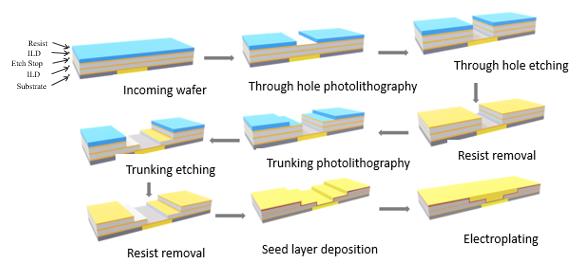
| Semiconductor electroplating equipment |
Copper interconnection electroplating equipment for the front end | Aiming at Ultra ECP map of the copper interconnection electroplating technology for the front end, which is the 55nn, 40nm, 28nm and below 20-14 nm technology nodes, the equipment mainly acts on the wafer to deposit a layer of dense and uniformly distributed copper without holes, gaps and other defects. | It can be used in the dual damascene electro-coppering process in logical circuits and memory circuits. |
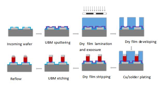
Advanced packaging electroplating equipment for the back end | The equipment is developed in a differentiated manner to meet the needs of advanced packaging electroplating and can be used for high-current and high-speed electroplating applications. It adopts a modular design, which is convenient for maintenance and control, can shorten the maintenance time of equipment and improve the utilization rate of equipment. | It can be used in the advanced packaging Pillar Bump, RDL, HD Fan-out and TSV, and the electroplating processes, such as copper, nickel, tin, silver, gold, etc. |
| Advanced packaging wet equipment |
| The equipment uses a single-chip cavity to perform wet etching on the wafer surface. It integrates all the chemical liquid, pure water and gas lines for drying in a complete process into a
| It can be used for wet silicon etching of 12-inch and 8-inch wafers and UBM metal wet etching processes in advanced packaging, such
|
| Advanced packaging wet equipment | cavity. The equipment occupies a small area, consumes less chemicals and pure water with high flexibility in process adjustment. | as copper, titanium, nickel, tin, gold, etc. |
Gumming equipment | The equipment uses a single-chip cavity to perform the photoresist spin coating on the surface of the wafer, and completes the subsequent roasting and cooling working procedure in the hot and the cold plate. The equipment pioneers the self-cleaning function of the cavity, which replaces the traditional manual disassembly of the cavity for cleaning, avoiding the damage to the machine caused by frequent manual disassembly of the precision gumming machine. At the same time, the cleaning efficiency is greatly improved, the maintenance cost of the machine is reduced, and the service life of the machine is increased. | It can be used for the coating process of positive and negative glue and thin and thick glue for 12-inch and 8-inch wafers in advanced packaging. |
Developing equipment | The equipment uses a single-chip cavity to spray the developing solution on the surface of the wafer, and cleans and dries the wafer after spraying the developing solution. The equipment combines the developing technology of Spray and puddle. | It can be used for the developing process of 12-inch and 8-inch wafers in advanced packaging. |
Degumming machine | The equipment integrates slot-type degumming with single-chip degumming, completes the soaking process in the slot, softens and removes most of the thick glue. The single-chip degumming can complete the subsequent removal of residual glue, contaminants and particles and make up for the shortcomings of insufficient capacity of single-chip equipment. | It can be used for the degumming process of 12-inch and 8-inch wafers in advanced packaging. |
Advanced packaging scrubbing equipment | The equipment uses a single-chip cavity to spray chemical liquid or deionized water on the front and back of the wafer to achieve the cleaning, and use the physical brush to clean the wafer. | It can be used for the scrubbing and cleaning process of 12-inch and 8-inch wafers in advanced packaging. |
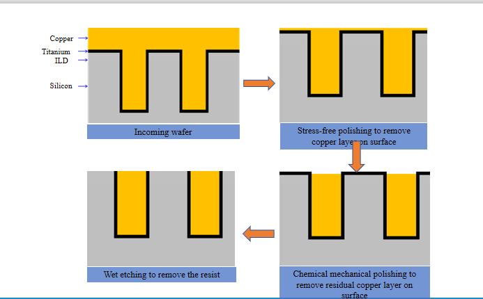
Stress-free polishing equipment | Stress-free polishing machine (Ultra SFP) is based on the principle of electro-chemistry and integrates stress-free polishing, chemical mechanical polishing, and wet etching processes. In advanced packaging applications, it can greatly reduce the consumption of polishing solution and reduce chemical emissions. | It can be used for 3D TSV, 2.5D silicon interposer, RDL, HD Fan-out, and others in advanced packaging. |
| Other equipment |
Vertical furnace tube equipment | The equipment can handle wafers process in batches to complete the deposition process of different types of non-metal thin films on the surface of wafers. It is mainly used for polycrystalline silicon, silicon nitride, silicon oxide and other thin films. | It can be used for the film deposition of polycrystalline silicon, silicon nitride, and silicon oxide in front end process of logical circuits and memory circuits. |
| | 3. | Composition of main business income |
During the reporting period, the company’s main business income according to product composition is as follows:
Unit: RMB 10,000 Yuan
| Project | 2019 | 2018 | 2017 |
| Amount | Proportion | Amount | Proportion | Amount | Proportion |
Semiconductor cleaning equipment | 62,522.30 | 84.10% | 50,135.96 | 92.91% | 21,492.48 | 86.27% |
Among them: single-chip cleaning equipment | 55,099.52 | 74.12% | 50,135.96 | 92.91% | 21,492.48 | 86.27% |
Slot-type cleaning equipment | 4,801.36 | 6.46% | - | - | - | - |
Single-chip slot-type combined cleaning equipment | 2,621.43 | 3.53% | - | - | - | - |
Semiconductor
| 7,857.39 | 10.57% | 1,191.13 | 2.21% | - | - |
| electroplating equipment | | | | | | |
Advanced packaging wet equipment | 3,961.12 | 5.33% | 2,634.07 | 4.88% | 3,421.33 | 13.73% |
Total | 74,340.81 | 100.00% | 53,961.17 | 100.00% | 24,913.81 | 100.00% |
During the reporting period, the income from the single-chip cleaning equipment has accounted for a relatively high proportion and grew rapidly. This is the company’s main source of income. Besides, the company has successfully developed the first scrubbing equipment for front end, the first stress-free polishing equipment, and the first vertical furnace tube equipment, and they have entered the customer verification; during the reporting period, there is no sales revenue.
(Ⅱ) Main operation model
The company is mainly occupied in the research, development, production and sales of semiconductor special equipment. It achieves revenue and profits through selling customized semiconductor cleaning equipment, semiconductor electroplating equipment, stress-free polishing equipment, vertical furnace tube equipment and advanced packaging wet equipment to wafer manufacturing, advanced packaging, semiconductor silicon wafer manufacturing enterprises, research institutes and other customers, and providing services.
As a company specializing in semiconductor equipment that faces the forefront of international technology and adheres to independent innovation, the company follows global industry practices. It is mainly focused on technology and process research and development, product design and manufacturing, and provides customers with equipment and process solutions. The company hardly engages in the processing of parts and components. According to the product design, the company has organized outsourcing of parts and external assistance, and has established a complete supply
chain system in the United States, South Korea and Chinese Mainland, and has developed a close cooperative relationship with core suppliers to guarantee the supply of important parts. With the help of the technological advantages formed through long-term research and development accumulation, the company maintains a higher product gross profit, and thus maintains a higher proportion for research and development investment and market development, and has achieved a higher profit margin during the reporting period.
| | 2. | Research and Development model |
The company mainly adopts the model of independent research and development. The research and development department of the company is guided by the international technical tendency of semiconductor special equipment and customer demands, adopts a strategy of differentiated competition, and relies on the international research and development teams with rich experience to develop new process and technologies, complete the verification of technical solutions, and has applied for patent protection in the major semiconductor production countries and regions in the world, and has quickly industrialized research and development results and achieved a series of technological innovations and breakthroughs. Besides, the company has established a professional research and development team in South Korea, relying on South Korea’s advantages in the field of semiconductor machinery and electronics, to develop related technologies for the company’s products and improve the company’s product performance.
The “Management Measures for the Research and Development Project” formulated by the company stipulates the procedures for the establishment, approval, and execution of research and development projects. On the basis of functional categories, the company divides research and development personnel into four categories: process development, mechanical design, electrical design, and software programming. Among them, the process development and mechanical design department is responsible for the process development and mechanical design of the process module, and the electrical design and software programming department is responsible for the automatic control design and control software programming of the equipment. After completing the project initiation and approval process of the research and development project, the company will create the technical plan and complete the product design; complete the manufacturing of new product according to the design. After the product has passed the company’s test, it will be sent to the customer for testing in the actual production environment. The company will continue to improve product performance based on customer feedback until the product is officially finalized. Among them, in respect of part of the testing work for the new product on the client, the company also needs to pay test development fee.
There are many kinds of raw material purchased by the company, and the main categories are gas circuit, materials conveying, machinery, the electrical, etc. The specific material includes robot arms, megasonic generators, filters, valves, sensors, etc.
In order to ensure the quality and performance of the product, the company has established a complete procurement system, requiring suppliers to fill out the “Supplier Survey Table”, establishing supplier files to figure out the situation of the supplier, such as personnel situation, production capacity, design capacity, financial situation, suppliers of key components, production and testing equipment, etc. And conduct comprehensive evaluation of the supplier’s product technology and quality, capacity of delivery just-in-time and after-sales service, etc., and finally determine the qualified supplier and put them into the list of qualified suppliers. At present, the company has established stable long-term cooperation with major suppliers.
The company has organized procurement teams for raw material in South Korea and the United States, and established ACM KR and ACM CA. They rely on the relatively developed and complete semiconductor industry chains in South Korea and the United States, and are responsible for the overseas procurement of some of the company’s raw materials.
According to the customer demands, the performance and indicators of raw
materials required by the products, the research and development and design engineers of the company inquire with suppliers based on the design drawings, and sign the “Procurement Demand Sheet”, and send it together with the supplier’s offer and design drawings to the purchasing department. After comprehensively taking the company’s current production plans, sales orders, raw material inventory, and other factors into account, the purchasing department arranges procurement plans, conducts business negotiations with suppliers, and finally determines the purchase price and trade terms. After obtaining the approval of the research and development and design department, purchasing department and financial department, select the supplier from the list of qualified suppliers as required and conduct the procurement. After the purchased materials are delivered, the quality control department conducts the receiving inspection. After passing the inspection, the warehouse clerk will go through the storage procedures and complete the purchase.
The company’s products are all based on the customized design and manufacturing according to the customer’s differentiated demands, and the company mainly adopts the production model where the sales volume determines the production, and organizes production in line with customer orders.
On the basis of market forecasting and non-binding forecasting from the customers, the company’s manufacturing department prepares annual production plans, and formulates monthly production plans based on customer orders. The research and development and design engineers provide assembly drawings according to the customer orders and distribute them to warehouses and production workshops for warehouse picking, batching and assembly. After the pre-assembly and pre-examination, each module is handed over to the production line for assembly and functional testing. After passing the test, it will be off line and delivered.
The cavity frames of the company’s products mainly consist of a variety of plastic parts and is produced by outsourcing processing. According to the differentiated demands of customers, the company hands over to outsourcing manufacturers for processing after completing the design. After passing the acceptance, the products are put into storage for production and assembly. The outsourcing manufacturers of the company have independent and mature processing capabilities. Outsourcing processing adopts standardized technology, and is performed according to the product technical parameters listed in the agreement or order. The company will strictly control the quality of outsourcing processing, and has established a stable cooperative relationship with outsourcing manufacturers for many years to ensure that it meets the differentiated needs of customers.
Since its establishment, the company has always adhered to the global development strategy. Customers are mainly located in Chinese Mainland, Taiwan, South Korea and other countries and regions.
The company’s market development strategy is:first of all, to develop the global leading semiconductor enterprises, and obtain their recognition for the company’s technology and products through long-term research and development and technology accumulation to establish the company’s market reputation. Then, with its achievements and reputation in the international industry, the company will continuously explore the emerging regional markets in the semiconductor industry, such as Chinese Mainland, etc. After years of hard work, the company has established a relatively stable cooperative relationship with Hynix, Yangtze Memory, Huahong Group, SMIC, JCET and other domestic and foreign leading enterprises in the semiconductor industry.
The company’s sales department will jointly discuss the product program with the mechanical design department, process department, electrical department, software department and after-sales department after receiving the customer’s order. The production department is responsible for organizing the production according to the design plan. After the product is qualified upon testing, it is shipped to the customer for installation, commissioning and acceptance. During the reporting period, the company has provided products to customers for testing before signing a formal sales
order in a few cases. After the product meets the technical specifications of the customers, both parties sign the official order.
The company sells products through the direct selling model, and there is no distribution and dealer model. During the reporting period, the company obtains orders through agent promotion, business negotiation with potential customers or bidding.
The sales cycle of semiconductor special equipment industry is long and there is a lot of uncertainty. In the early stage of the development, the company’s business scale is too small to cover many potential customers. The company mainly develops the market through agents. With the continuous expansion of the company’s business scale, the company also begins to expand its sales team. Under the agent promotion, the company signs a product sales agency agreement with the agent, and the agent is responsible for the marketing of related products in a specific region. The company directly signs sales contracts with relevant customers, and directly sends the products to customers, and pays the commission charges to the agent in accordance with the types of the sold products and the commission rate agreed in advance.
In 2017 and 2018, part of the company’s export business was carried out by the import and export service provider, Charter Base International. The specific method was to sell the product to Charter Base International at first, which would go through customs procedure and then Charter Base International would sell the products to the final customers at the same price. At the same time, the company would pay Charter Base International for the agency fees of customs procedure. After June 2018, the company’s export business was carried out through the wholly-owned subsidiary, Hong Kong CleanChip, and the company no longer had business with Charter Base International.
6. Reasons for adopting the current business model, key factors affecting the business model, changes and future trends of the business model and influencing factors during the reporting period
Combined with factors such as market supply and demand, upstream and downstream development status, industrial policies, the company’s main business, main products, core technologies, and its own development stage, the company has formed its current business model. The business model is consistent with the practice in the same industry. The business model and its influencing factors of company have not faced major changes during the reporting period, nor will there be major changes of business model in the foreseeable future.
(Ⅲ) Evolution situation of the company’s main business, main products or services, main business model since its establishment
| | 1. | Evolution situation of the company’s main business and products |
Since its establishment, the company has always focused on the research and development, production and sales of semiconductor special equipment. The company’s controlling shareholder, ACMR, was established in 1998. Since its establishment, ACMR has been engaged in the research and development of semiconductor special equipment. In 2005, ACMR invested and set up the company’s predecessor, ACMSH, and put the right to use the technology related to semiconductor special equipment to ACMSH, which was formed from its previous research and development. On the basis of these technologies, the issuer carries out continuous technology development and innovation, and conducts technology research and development and technology accumulation of semiconductor special equipment.
Among the company’s technology and product lines, semiconductor cleaning equipment has achieved market breakthrough at first. In 2008, the SAPS technology of the company was successfully developed. In 2009, the SAPS cleaning equipment entered the product verification of the world’s top ten semiconductor companies and the global leading enterprise for memory, Hynix. In 2011, the company got the official order from Hynix for the first time owing to the SAPS cleaning equipment for 12-inch 45nm process, and received repetitive orders of Hynix in 2013. In the field of semiconductor cleaning equipment, the company has successfully entered the
production line of the world’s first-rate semiconductor manufacturing enterprises after more than ten years of research and development and technical accumulation.
After 2015, the semiconductor industry in Chinese Mainland has entered a period of rapid development, and the demand for semiconductor special equipment has increased rapidly. Since the company’s production rate was firstly recognized by international advanced customers, the company has successfully obtained orders from leading customers in Chinese Mainland after 2015 with its achievements and reputation in the international industry, such as Yangtze Memory, SMIC, and Huahong Group. In 2015 and 2018, the TEBO technology and Tahoe technology of the company were successfully developed respectively, and the technology and product line in the field of semiconductor cleaning equipment were more colorful. During the reporting period, the company firmly grasped the opportunities for the rapid development of the semiconductor industry in Chinese Mainland. The business scale of semiconductor cleaning equipment grows rapidly.
In the field of advanced packaging wet equipment, after years of technology accumulation, the company obtained the order of JCET, which was the leading enterprise in the domestic packaging and testing field, in 2013.
Advanced packaging electroplating equipment for the back end and stress-free polishing equipment are one of the company’s early business directions. After years of research and development and marketing, the company respectively obtained the orders of JCET in 2018 and 2019. The company got the orders of Huahong Group in 2019 owing to the copper interconnection electroplating equipment for the front end.
In order to further expand the company’s market coverage of semiconductor special equipment, the company began the research and development of dry equipment based on the wet process in 2018, and launched vertical furnace tube equipment in 2020, which further enriches the company’s product line and expands the market areas covered by the company’s products.
Since its establishment, the company’s main business has not changed. The evolution situation of the company’s main products is as follows:
2. The evolution situation of the company’s main operation model
Since its establishment, the company’s operation model has not changed.
(Ⅳ) Process flow of main products
The industry of semiconductor special equipment is a technology-intensive industry, and the production technology involves the comprehensive application of multi-disciplinary and multi-domain knowledge such as microelectronics, electrical science, machinery, materials, chemical engineering, fluid mechanics, automation, image recognition, communication, and software systems. The production process flow of the company’s various products is similar in some places. The specific process flow is as follows:
(V) Main environmental pollutants, main treatment facilities and treatment capacity involved in production and operation
The company is mainly engaged in the research, development, production and
sales of semiconductor special equipment. The main production process is the assembly, detection and debugging of machinery equipment and modules, and there is no serious pollution.
At present, the main environmental protection measures taken by the company in the process of research and development and production are as follows:
1. During the research and development period, there is a small amount of pollutants. The waste water with fluorine, acid, alkali and other components will be collected and entrusted to a qualified third-party company for transportation and disposal.
2. The company’s domestic sewage is directly discharged into the municipal sewage pipe network. After the collected water for cleaning equipment has passed through the recycling system and reached the standard, it will be directly discharged into the municipal sewage pipe network. Domestic waste is handled by the sanitation department. The solid wastes are collected in a unified manner, and then they are entrusted to professional units for disposal.
3. The company’s workshop is equipped with a ventilating system for exhausting air. The equipment has basic vibration reduction, noise elimination and sound insulation devices to reduce noise emissions.
Ⅱ. The basic situation and competition condition of the issuer’s industry
(Ⅰ) The company’s industry and the basis for determining the industry
The company is mainly occupied in the research, development, production and sales of semiconductor special equipment. According to the “Guidelines for the Industry Classification of Listed Companies (2012 Revision)” issued by the China Securities Regulatory Commission, the company’s industry is “Special Equipment Manufacturing” (C35); according to the “Classification of National Economy Industry” (GB/T4754-2017), the company’s industry is “Special Equipment Manufacturing for semiconductor devices” under “Special Equipment Manufacturing” (C3562).
(Ⅱ) The competent authority of the industry, the supervision mechanism of the industry, the main laws, regulations and policies of the industry and its influence on the operation and development of the issuer
| | 1. | The competent authority and supervision mechanism of the industry |
The competent authority of the semiconductor special equipment industry where the company is located is the Ministry of Industry and Information Technology and the Ministry of Science and Technology. The industry’s self-regulatory organizations are China Semiconductor Industry Association and China Electronic Production Equipment Industry Association.
The main responsibilities of the Ministry of Industry and Information Technology are as follows: put forward new industrialization development strategies and policies, coordinate and solve major problems in the process of new industrialization, formulate and organize the implementation of development plans for industry, communications industry and informatization, and promote strategic adjustment, optimization and upgrading of industrial structure;To formulate and organize the implementation of industry plans, plans and industrial policies for industry and communications; monitor and analyze the operation situation of the industry and communication industry, make statistics and release relevant information, and conduct forecast and warning and information guidance; formulate and organize the implementation of industry plans, programs and industrial policies for industry and communications; supervise and analyze the operation trend of industry and communication industry, carry on the statistics and release relevant information, and conduct prediction and early warning and information guidance; burden the responsibility for proposing opinions on the scale and direction of investment in fixed assets in industry, communications industry and informatization (including the utilization of foreign capital and overseas investment),
and the arrangement ideas on fiscal construction funds from the central government, and reviewing and approving the fixed assets investment projects within Chinese planning and the annual planned scale in accordance with the limits of authority prescribed by the State Council; formulate and organize the implementation of plans, policies and standards related to the information industry in the high-tech industry, and guide the technological innovation and technological progress in the industry, and upgrade traditional industries with advanced and applicable technologies; burden the responsibility for the organization and coordination of the revitalization of the equipment manufacturing industry, organize and formulate plans and policies for major technological equipment development and independent innovation, rely on the construction of key national projects to coordinate the implementation of major special projects, promote the localization of major technical equipment and guide and introduce the learning and innovation of major technical equipment.
The main responsibilities of the Ministry of Science and Technology are as follows: formulate Chinese innovation-driven development strategy, scientific and technological development, introduce and implement the foreign intellectual planning and policies; be responsible for establishing a unified management platform of Chinese science and technology and the coordination, evaluation and supervision mechanism of the fund for scientific research project; formulate and carry out Chinese basic research plans, policies and standards; compile the major science and technology projects in China and supervise the implementation; formulate relevant policies and measures for the conversion of scientific and technological achievements and the cooperation of industry, university and research, and supervise the implementation.
China Semiconductor Industry Association and China Electronic Production Equipment Industry Association are mainly responsible for implementing government industrial policies; performing industry and market research and providing consulting services to member units and government authorities; self-discipline management of the industry; propose industrial development suggestions and opinions to government departments on behalf of the member units.
The Ministry of Industry and Information Technology, the Ministry of Science and Technology and industry associations constitute the management system of the semiconductor equipment industry. Under the macro control of the competent authority and the constraints of self-disciplining norms of the industry associations, enterprises in various industries runs independently in the market and assume market risks by themselves.
| | 2. | The main laws, regulations and policies of the industry and its influence on the operation and development of the issuer |
The semiconductor special equipment industry of the company is the key industry of which China focuses on encouraging development. In order to enhance the development, innovation capacity and international competitiveness of the semiconductor industry, promote the transformation of traditional industries and product upgrading and updating, and further propel the sustained, rapid and healthy development of the national economy, the central and local governments of China have launched a series of policies in recent years, such as “Development Guidelines for Information Industry” and “Several Measures for the Concentrated Development of Integrated Circuit Industry in Lingang New Area of China (Shanghai) Pilot Free Trade Zone”, to encourage and support the development of the semiconductor industry, which has created a good policy environment for the development of the semiconductor industry, and promoted the development of the semiconductor special equipment industry in Chinese Mainland.
(III) Development Situation of the Issuer’s Industry in Terms of New Technologies, New Industries, New Patterns, New Models, Etc. over the Past Three Years and the Future Development Trend
(1) Overview of the semiconductor industry
Semiconductors refer to materials with conductivity ranking between conductors and insulators at room temperature and are widely used in various electronic products.
Semiconductor products can be divided into four categories: integrated circuits (IC), discrete devices, optoelectronic devices and sensors. As the core of the semiconductor industry, integrated circuits account for more than 80% of the scale of the semiconductor industry, and the subdivisions include logic chips, storage, microprocessors, analog chips, etc. Integrated circuits are widely used in 5G communication, computer, consumer electronics, network communication, automobile electronics, Internet of Things (IoT) and other industries, and are the core component of most electronic equipment.
From the perspective of the industry chain, the semiconductor industry chain involves supporting industries such as materials and equipment, chip design, wafer manufacturing, packaging & testing industry and semiconductor product terminal application industry. Semiconductor products represented by integrated circuits are widely used, and the demand growth in downstream application industries is the core driving force for the rapid development of the semiconductor industry.
Semiconductor industry chain
| ① | The market scale of the global semiconductor industry is large |
With the rapid development of global informatization, networking and knowledge economy, especially driven by the strong demand of emerging application fields such as IoT, artificial intelligence (AI), automotive electronics, smartphones, smart wear, cloud computing, big data and security electronics, the revenue of the global semiconductor industry is enormous. In 2018, the revenue of the global semiconductor industry reached USD 476.151 billion dollars. In 2019, due to the impact of the global macro-economic doldrums, the prosperity of the semiconductor industry declined, and the revenue of the global semiconductor industry fell to USD 419.148 billion dollars, down 11.97% year on year. The semiconductor industry is expected to recover in 2021, and the revnue of the global semiconductor industry is expected to reach USD 572.788 billion dollars in 2024. According to Gartner’s statistics and forecasts, the revenues of the global semiconductor industry and annual growth rate from 2018 to 2024 are as follows:
Revenues and annual growth rates of the global semiconductor industry for 2018-2024
Data source: Gartner
| ② | Integrated circuits are the most important component of the semiconductor industry. |
The semiconductor industry can be divided into four product categories: integrated circuit, optoelectronic device, discrete device and sensor. In 2018, the global sales of integrated circuits, optoelectronic devices, discrete devices and sensors were USD 393.288 billion, 38.032 billion, 24.102 billion and 13.356 billion, respectively, up 14.60%, 9.25%, 11.32% and 6.24% from 2017, accounting for 83.90%, 8.11%, 5.14% and 2.85% in the global semiconductor industry. In terms of the product distribution of the semiconductor industry, the proportion of integrated circuits is the highest and the growth rate is the fastest. Integrated circuits are the most important component of the semiconductor industry.
Product distribution of the global semiconductor industry in 2018
Data source: WSTS
| ③ | The global semiconductor industry is expected to continue to shift towards mainland China in the future |
In the development history of the global semiconductor industry, we’ve seen several rounds of industrial shift from the United States to Japan, South Korea, Taiwan (China), and mainland China. At present, mainland China is in the process of the rapid rise of the new generation of smartphones, IoT, AI, 5G communication and other industries, and has become one of the most important semiconductor application and consumer markets in the world. According to the statistical data from the Semiconductor Equipment and Materials International (SEMI), 62 new wafer factories will be put into operation in the world from 2017 to 2020, of which 26 will be located in mainland China, accounting for 42%. The period from establishment to production of new wafer plants is about 2 years, and the next few years will be the rapid development period of the semiconductor industry in mainland China.
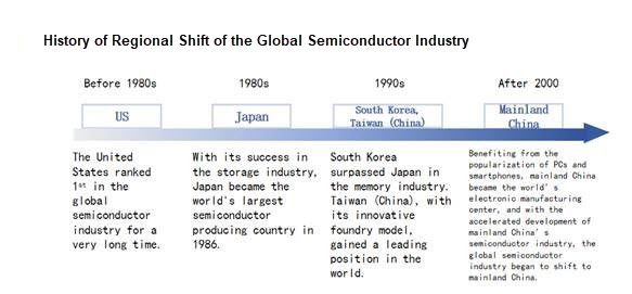
Against the backdrop of regional migration of the global semiconductor industry, according to WSTS statistics, in 2018, the global shares of semiconductor markets in Asia-Pacific (excluding Japan), the United States, Europe and Japan were 60%, 22%, 9% and 9% respectively; in 2018, the U.S. semiconductor market grew by 19.6%, Europe by 13.3%, Japan by 9.6% and Asia-Pacific by 16.0%, of which the growth rate in mainland China was 20%. With the rapid growth of China’s semiconductor market, its global position is also rising rapidly. In 2019, while the growth rate of the global semiconductor market declined, the semiconductor market in mainland China still grew faster than the global market, thereby driving the Asia-Pacific region to become the fastest-growing semiconductor market in the world. In 2017-2019, the sales percentage
and growth rates of semiconductor markets in all countries or regions in the world were as follows:
| Country/Region | 2019 (E) | 2018 | 2017 |
Sales Percentage | Growth | Sales Percentage | Growth | Sales Percentage | Growth |
| US | 21.90% | 1.44% | 22.14% | 19.58% | 21.47% | 35.03% |
| Europe | 9.02% | 1.95% | 9.08% | 13.25% | 9.29% | 17.13% |
| Japan | 8.39% | 2.52% | 8.39% | 9.58% | 8.88% | 13.33% |
| Asia-Pacific | 60.69% | 3.06% | 60.39% | 16.00% | 60.36% | 19.40% |
| Mainland China | 32.37% | 3.50% | 32.08% | 16.60% | 31.90% | 22.10% |
| Total | 100.00% | 2.55% | 100.00% | 15.94% | 100.00% | 21.62% |
Data source: Shanghai IC Industry Development Report 2019, Economic and Information Technology Commission of Shanghai, Shanghai Integrated Circuit Industry Association
| ④ | China’s semiconductor industry continues to grow rapidly |
Relying on the large market demand of terminal applications in China, the scale of the semiconductor industry in mainland China continues to grow, especially the development of the integrated circuit industry. According to data released by China Semiconductor Industry Association (CSIA), the sales scale of the integrated circuit industry in mainland China was RMB 250.85 billion Yuan in 2013, RMB 653.20 billion Yuan in 2018 (up by 20.71% year-on-year), and RMB 756.23 billion Yuan in 2019 (up by 15.77% year-on-year). From 2013 to 2019, the annual compound growth rate of the sales scale of the integrated circuit industry in mainland China was 20.19%, developing rapidly.
4
Sales and growth rates of China’s IC industry for 2013-2019
In the industry chain structure of the integrated circuit industry in mainland China in 2019, the sales revenue of the chip design industry was RMB 306.350 billion Yuan, up by 21.60% year-on-year; the sales revenue of the wafer manufacturing industry was RMB 214.910 billion Yuan, up by 18.20% year-on-year; the sales revenue of the packaging & testing industry was RMB 234.970 billion Yuan, up by 7.10% year-on-year. In each link of the above semiconductor industry chain, the rapid growth of wafer manufacturing sales revenue is mainly attributed to China’s a batch of 12-inch and 8-inch wafer manufacturing production lines put into production in recent years. Besides, with the development of the chip design industry at home and abroad, the wafer manufacturing industry in Chinese Mainland has been growing fairly fast.5
Sales and growth rates of China’s IC industry chain structure for 2014-2019
Unit: RMB 100mn Yuan
4 Data source: Shanghai IC Industry Development Report 2019, Economic and Information Technology Commission of Shanghai, Shanghai Integrated Circuit Industry Association, and China Semiconductor Industry Association
5 Data source: Shanghai IC Industry Development Report 2019, Economic and Information Technology Commission of Shanghai, Shanghai Integrated Circuit Industry Association, and China Semiconductor Industry Association
| Year | 2019 | 2018 | 2017 | 2016 | 2015 | 2014 | 2014-2019 Compound Growth |
| Chip design | Sales | 3,063.50 | 2,519.3 | 2,073.5 | 1,644.3 | 1,325.0 | 1,047.4 | 23.94% |
| Growth | 21.60% | 21.5% | 26.1% | 24.1% | 26.5% | 29.5% |
| Wafer manufacturing | Sales | 2,149.10 | 1,818.2 | 1,448.1 | 1,126.9 | 900.8 | 712.1 | 24.72% |
| Growth | 18.20% | 25.6% | 28.5% | 25.1% | 26.5% | 18.5% |
| Packaging & testing | Sales | 2,349.70 | 2,193.9 | 1,889.7 | 1,564.3 | 1,384.0 | 1,255.9 | 13.35% |
| Growth | 7.10% | 16.1% | 20.8% | 13.0% | 10.2% | 14.3% |
| Total | Sales | 7,562.30 | 6,531.4 | 5,411.3 | 4,335.5 | 3,609.8 | 3,015.4 | 20.19% |
| Growth | 15.78% | 20.7% | 24.8% | 20.1% | 19.7% | 20.2% |
(2) Overview of the semiconductor special equipment industry
| ① | Classification of semiconductor special equipment |
Semiconductor special equipment generally refers to the production equipment required for the production of various semiconductor products. It is part of the supporting link of the semiconductor industry chain. Semiconductor special equipment is the technical leader of the semiconductor industry. Chip design, wafer manufacturing and packaging & testing need to be designed and manufactured within the scope allowed by equipment technologies. The technological progress of equipment in turn promotes the development of the semiconductor industry. Take the integrated circuit, which is of the greatest technological difficulty, the most added value, and the most complex technology in the semiconductor industry chain as an example, the production equipment used for integrated circuits can be divided into two categories, the front-end process equipment (wafer manufacturing) and the back-end process equipment (packaging & testing). Among them, there are seven process steps in the front-end wafer manufacturing, including thermal process, photo-lithography, etch, ion implantation, dielectric and metal deposition, cleaning & CMP, and metallization. The corresponding dedicated equipment mainly includes oxidation/diffusion equipment, photolithography equipment, etching equipment, cleaning equipment, ion implantation equipment, film deposition equipment, mechanical polisher, etc.
The main types of equipment used for integrated circuit manufacturing are as follows:
| ② | Characteristics of the semiconductor special equipment industry |
A. Semiconductor special equipment plays an important role in the semiconductor industry chain
Semiconductor special equipment plays an important role in the semiconductor industry chain. The technology of semiconductor special equipment is complex, and customers have strict requirements on the technical parameters and operation stability of the equipment in order to ensure the production efficiency, quality and yield.
According to Moore’s law, when the price remains unchanged, the number of components that can be accommodated on an integrated circuit will double every 18 to 24 months, and the performance will also double. Accordingly, the equipment supplier in the integrated circuits industry must also introduce more advanced manufacturing processes every 18 to 24 months; the technological progress of the integrated circuit manufacturing process in turn promotes the semiconductor special equipment enterprises to continuously pursue technological innovation. In the meantime, the technology update iteration of the integrated circuit industry also brings continuous demand for equipment investment, and the technological improvement of semiconductor special equipment also boosts the sustained and rapid development of the integrated circuit industry.
B. The technical barriers for semiconductor special equipment is high, and it is hard to pass customer verification
The industry of semiconductor special equipment is a technology-intensive industry, and its production technology involves the comprehensive application of knowledge in numerous disciplines and fields, such as microelectronics, electric, mechanical, material, and chemical engineering, fluid mechanics, automation, image recognition, communication, software system, etc. Global giants in the semiconductor special equipment industry have a rather high market share, especially in photolithography equipment, detection equipment, ion implanter, and other fields, where they enjoy monopoly. Moreover, they have taken intellectual property protection measures in most technical fields. Therefore, the technical barriers for semiconductor special equipment industry is vary high. A small number of enterprises in Chinese mainland have made technological breakthroughs and innovations in some fields after more than ten years of technology R&D and process accumulation, and have successfully launched differentiated products on the premise of avoiding intellectual property disputes, which have been recognized by customers at home and abroad and have gradually entered the international market.
Semiconductor special equipment has high value and complex technology, which has a huge impact on the product quality and production efficiency of downstream customers. Customers in the semiconductor industry have strict requirements for the quality, technical parameters and stability of semiconductor special equipment, and they are also very cautious in selecting new equipment suppliers. Usually, they select suppliers with a certain level of market reputation and market share in the industry, and carry out a long-cycle equipment verification process. Generally, customers in the semiconductor industry require equipment suppliers to provide products for testing, and then they will be included in the list of qualified suppliers after passing their internal verification; some customers still need to send the semiconductor products produced by using such equipment to their downstream customers, and only after obtaining the approval of their customers can equipment suppliers be included in the list of qualified suppliers. Therefore, semiconductor special equipment enterprises face a long time cycle and great difficulty in customer verification and market exploration.
| | ② | Upstream and downstream industries of the semiconductor special equipment industry |
The upstream industry of the semiconductor special equipment industry is the electronic component and machining industry. The raw materials purchased are mainly robot arms, megasonic generators, filters, valves, sensors, etc. Because of the characteristics of high precision and high reliability of semiconductor special equipment, the requirements for raw materials and parts are correspondingly high.
The downstream industries of the semiconductor special equipment industry are mainly wafer manufacturing, packaging & testing industries, etc. In particular, integrated circuit products have high technology content and complex processes, and technological updates and process upgrades rely on the development of special equipment; in turn, the continuous development of new products and processes in the downstream industries provides new demand and market space for the equipment industry. Taking wafer manufacturing as an example, manufacturing equipment applicable for 8-inch wafer cannot be used to process 12-inch wafer. Therefore, when the integrated circuit industry enters the 12-inch era, the manufacturing equipment
applicable for 8-inch wafer needs to be completely updated. Additionally, as the wafer manufacturing technology and process continuously develop towards high precision and high integration, more advanced technologies and processes also require improvement and upgrading of the equipment technolog, which in turn will brings incremental space for the equipment industry.
| ③ | Situation of the semiconductor special equipment industry |
A. Downstream market demand drives the continuous scale growth of the global semiconductor special equipment industry
The market of semiconductor special equipment is closely related to the prosperity of the semiconductor industry, among which the chip manufacturing equipment is the field with the most demand in the semiconductor special equipment industry. According to Gartner’s statistics, the total equipment expenditure of chip manufacturers in the world in 2018 reached USD 58.944 billion, and it is expected to decline slightly to USD 55.480 billion in 2019 as a result of the global macroeconomic downturn. The semiconductor industry is expected to recover in 2021, and will grow to USD 60.214 billion in 2024. From 2020 to 2024, the compound annual growth rate is expected to be 6.27%.
Data source: Gartner
In the future, with the steady growth of downstream industries such as 5G communication, computers, consumer electronics, network communications, etc., as well as the rapid development of emerging industries such as IoT, AI, automotive electronics, smart phones, smart wearables, cloud computing, big data and security electronics and other emerging fields, the integrated circuit industry will face the demand for capacity expansion of new chips or advanced processes, which will bring broad market space for the semiconductor special equipment industry.
In integrated circuit equipment, chip manufacturing equipment is the core equipment with the highest technical requirements, the most difficult manufacturing and the highest value. The technical difficulty, value and market share of semiconductor special equipment are in direct proportion. According to statistics from SEMI, from previous sales, the front-end manufacturing equipment accounts for about 80% of the market of semiconductor special equipment, and the back-end packaging & testing equipment accounts for about 20%. Photolithography, etching and cleaning, film deposition, ion implantation, process control and detection devices are the key process equipment. The value of these process devices accounts for a relatively high proportion of the cost of a single production line in the wafer factory.
Investment proportions for main IC devices
Data source: SEMI, Issue 4 of the Semiconductor Equipment Topic: The Year of Deployment –Looking for Invisible Leaders, GF Securities, April 2018
B. Foreign manufacturers dominate the global semiconductor special equipment market, and the degree of industrial concentration is high
The semiconductor special equipment industry has high technical barriers, market barriers and customer recognition barriers. After years of development, well-known global enterprises such as Applied Material (US), ASML (the Netherlands), LAM (US), TEL and DNS (Japan), and KLA (US) have occupied the main share of the global semiconductor special equipment market by virtue of their advantages in capital, technology, customer resources, brand, etc. According to statistics from VLSI Research, the total sales volume of the top 5 semiconductor special equipment manufacturers in the world in 2018 was USD 52.784 billion, with a year-on-year growth of 17.73%. 6
In 2018, the market share of the top 10 semiconductor special equipment companies in the world reached 81%, and the market share of the top five semiconductor special equipment companies reached 71%, showing a high degree of market concentration.7
Rankings of Top 5 Semiconductor Equipment Manufacturers in the World for 2018
Unit: USD 100mn
| Ranking | Manufacturer | Main Product Fields | Sales |
| 1 | Applied Material | Deposition, etching, ion implantation, grinding, etc. | 140.16 |
| 2 | ASML | Photolithography equipment | 127.72 |
| 3 | TEL | Deposition, etching, developing, cleaning, etc. | 109.15 |
| 4 | LAM | Etching, deposition, cleaning, etc. | 108.71 |
| 5 | KLA | Detecting and measurement equipment | 42.10 |
| Total | | 527.84 |
Globally, Applied Materials, a US company, as the largest supplier of semiconductor special equipment, leads the world in heat treatment, coating equipment, ion implantation equipment and other key links of wafer manufacturing equipment; Japanese semiconductor companies do a better job at manufacturing etching equipment, cleaning equipment, coating equipment, developers, testing equipment and other products; ASML, a Dutch company, is in the leading position in the field of high-end photolithography equipment; LAM, a US company, has advantages in the field of etching, cleaning and electroplating equipment; as for semiconductor special equipment enterprises in mainland China, after years of rapid development, they are now capable of competing against global leading enterprises in the fields of etching equipment, cleaning equipment, packaging & testing equipment, etc.
C. The scale of the semiconductor special equipment market in mainland China is growing rapidly
With the shift of global semiconductor industrial chain to mainland China, the Chinese integrated circuit industry has been growing rapidly. According to Gartner’s statistics, in 2018, China’s chip manufacturers’ equipment expenditure reached USD 10.434 billion, and in 2019 it was USD 12.244 billion. It is expected that in 2020, affected by the global semiconductor industry’s recession transmission, it will decline to USD 9.628 billion, with the global semiconductor industry gradually recovering in 2021. In 2024, it will increase to USD 12.842 billion. From 2020 to 2024, the compound annual growth rate is expected to be 7.47%.
6 Data source: Shanghai IC Industry Development Report 2019, Economic and Information Technology Commission of Shanghai, Shanghai Integrated Circuit Industry Association
7 Data source: Strategies for the Semiconductor Equipment Industry for 2020, BOCI Securities, Dec. 2019
Scale of China’s semiconductor special equipment market for 2018-2024
Data source: Gartner
D. The development of semiconductor special equipment made in China is increasing
The chip manufacturing industry, especially the wafer manufacturing industry, often has a large scale of equipment investment. At present, the investment of 12-inch wafer manufacturing projects is billions or ten billions of US dollars. The technology of wafer manufacturing is complex, involving many process steps, and there are many kinds of equipment needed for production. The efficiency and reliability of a single piece of equipment will directly affect the work efficiency of the whole production line and the yield of chip products. Therefore, wafer manufacturing enterprises are very cautious about the selection of new equipment, requiring a long verification cycle. First, they want to ensure that the equipment is technically advanced and reliable, and then they will consider commercial conditions such as economy and decide whether to purchase the equipment or whether to apply the equipment in production.
In recent years, as China attaches great importance to the semiconductor industry, some Chinese semiconductor special equipment enterprises have made breakthroughs in some technical fields after more than ten years of technology research and development and accumulation, and have successfully passed the verification of some integrated circuit manufacturing enterprises, becoming equipment suppliers of manufacturing enterprises.
Sales and growth rates of China’s domestic semiconductor special equipment for 2014-2019
Data source: 2019 Shanghai Integrated Circuit Industry Development Research Report, Shanghai Economic and Information Technology Commission, Shanghai Integrated Circuit Industry Association.
Although the sales volume of Chinese semiconductor special equipment enterprises keeps growing, the overall domestic production rate is still relatively low. At present, China’s semiconductor special equipment mainly relies on imports. According to statistics from China Electronic Production Equipment Industry Association (CEPEA), the sales volume of domestic semiconductor special equipment in 2018 was RMB 10.9 billion Yuan, with a self-sufficiency rate of about 13%. The self-sufficiency rate in the field of integrated circuit manufacturing equipment is even lower, so the development potential of Chinese semiconductor special equipment companies is significant.
According to the statistics of equipment purchase of mainland China’s major wafer factories, the localization of mainland China’s major wafer factories is as follows:
| SN | Equipment | Localization Rate | Major Domestic Manufacturers |
| 1 | Film stripping equipment | Above 90% | Beijing E-Town Semiconductor Technology Co., Ltd. |
| 2 | Cleaning equipment | About 20% | ACMSH, NAURA |
| 3 | Etching equipment | About 20% | AMEC, NAURA, Beijing E-Town Semiconductor Technology Co., Ltd. |
| 4 | Heat processing equipment | About 20% | NAURA, Beijing E-Town Semiconductor Technology Co., Ltd. |
| 5 | PVD equipment | About 10% | NAURA |
| 6 | CMP equipment | About 10% | Tianjin Hwatsing Electromechanical Technology Co., Ltd. |
| 7 | Film lamination and developing equipment | Breakthrough of zero | KINGSEMI |
| 8 | Photolithography equipment | Breakthrough of zero expected | Shanghai Micro Electronics Equipment (Group) Co., Ltd. (“SMEE”) |
Data source: Strategies for the Semiconductor Equipment Industry for 2020, BOCI Securities, Dec. 2019
To sum up, with the technological breakthroughs of some enterprises in China’s semiconductor special equipment industry, the development of this industry is expected to accelerate.
| ④ | Future development trend of the semiconductor special equipment industry |
A. Semiconductor special equipment will develop towards high precision and high integration
With the continuous advance of semiconductor technology, the integration degree of semiconductor devices is increasing. On one hand, the chip process nodes are shrinking, from 12 μm-0.35 μm (1965-1995) to 65 nm-22 nm (2005-2015), and they are still developing towards more advanced dimensions; on the other hand, the size of semiconductor wafer is expanding; the mainstream wafer size has developed from 4 inches and 6 inches to 8 inches and 12 inches at the current stage. In addition, the structure of semiconductor devices tends to be complex. A case in point is the NAND flash memory in the field of memory. According to the international semiconductor technology roadmap, when the process size reaches 14nm, the current flash memory technology will reach the limit of size reduction, and the memory technology will change from two-dimensional to three-dimensional architecture and enter the 3D era. In the manufacturing process of 3D NAND, the main task is to change the two-dimensional horizontal series storage units in 2D NAND into vertical ones. By increasing the number of 3D layers, we can solve the process problem of difficulty in 2D scale-down. The number of stacking layers is also developed from 32 and 64 layers to 128 layers. These requirements for the precision and stability of semiconductor special equipment are becoming higher and higher. In the future, semiconductor special equipment will develop towards high precision and high integration.
2D NAND and 3D NAND structure diagram
B. Coexistence and joint development of equipment of different technical grades
Given that the application of semiconductor chips is extremely wide, and the performance requirements and technical parameters vary widely, for example, SoC logic chips used in mobile phones often require 12-inch wafers and 7nm advanced processes. For industrial, automotive, and power electronics chips, 6-inch and 8-inch wafers and μm-level processes are still used in large numbers. The demand for chips of different technical levels coexist in large numbers, which also determines that there are market demands for semiconductor special equipment of different technical levels. With the continuous development of the semiconductor industry technology in the future, the demand for the semiconductor special equipment suitable for 12-inch wafers and with more advanced technology will grow at a faster speed, but the equipment of high, medium and low technological levels have their corresponding market space and will continue to coexist in the near future.
(3) Introduction to the market segment of the issuer’s main products
A. Importance of semiconductor cleaning in the chip manufacturing process
Cleaning is an important process link throughout the semiconductor industry chain. It is used to clean the impurities that may exist in each step of semiconductor silicon wafer manufacturing, wafer manufacturing, and packaging & testing in order to prevent impurities from affecting the high-yield rate of chips and the performance of chips. At present, with the chip manufacturing process becoming more and more advanced, the requirements for the control of wafer surface pollutants are getting higher, and after each repetitive process such as photolithography, etching, and deposition, a cleaning process is required.
Semiconductor cleaning refers to the non-destructive cleaning of the wafer surface to remove particles, natural oxide layers, metal pollution, organic matters, sacrificial layers, polishing residues and other impurities in the semiconductor manufacturing process. The categories, sources and main harm of pollutants in semiconductor cleaning are as follows:
| Pollutant | Source | Main Harm |
| Particles | Environment and other engineering processes | Affect the subsequent photolithography and dry etching processes, causing device short circuit. |
| Natural oxidation layer | Environment | Affect the subsequent oxidation and deposition processes, causing the electrical property to fail. |
| Metal pollution | Environment and other engineering processes | Affect the subsequent oxidation process, causing the electrical property to fail. |
| Organic matters | Dry etching byproducts and environment | Affect the subsequent deposition process, causing the electrical property to fail. |
| Sacrificial layer | Oxidation/deposition process | Affect specific subsequent processes, causing the electrical property to fail. |
| Polishing residues | Grinding fluid | Affect specific subsequent processes, causing the electrical property to fail. |
In order to ensure the yield and performance of the chip, the above-mentioned various contaminants on the surface of the wafer need to be controlled within the range of process requirements during the wafer manufacturing process. All wafer
manufacturing processes must be carried out in a strictly controlled purification environment. At the same time, it is necessary to evaluate whether the surface characteristics of the wafer meet the requirements of the process before each step. Currently, chip technology nodes are constantly improving, from 55nm, 40nm, 28nm to 14nm, 7nm and below, the requirements for the control of contaminants on the wafer surface are becoming higher and higher, and a cleaning process is required before and after repetitive processes such as photolithography, etching, and deposition Process.
In the semiconductor silicon wafer manufacturing process, the polished silicon wafer needs to be cleaned to ensure its surface smoothness and performance, thereby improving the yield in the follow-up process; in the wafer manufacturing process, it needs to be cleaned before and after photolithography, etching, deposition and other key processes to remove polluting chemical impurities on the wafer and reduce the defect rate; in the packaging stage, it needs to go through TSV cleaning, UBM/RDL cleaning, etc. based on the packaging process. The technical requirements of the aforementioned cleaning process are one of the most important factors affecting the chip yield, quality and reliability.
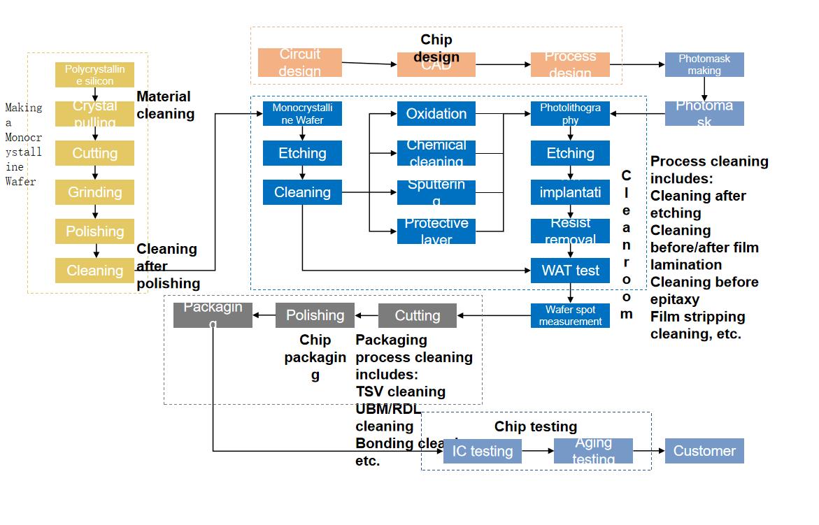
As wafer manufacturing process continues to develop towards higher precision, the complexity of the chip structure is increasing, and the sensitivity of chips to impurity content is also increasing accordingly. Small impurities will directly affect the yield of chip products. In the hundreds of chip manufacturing processes, a large number of small pollutants will inevitably be generated or contacted. In order to minimize the impact of impurities on chip yield, the current chip manufacturing process has set up a cleaning process after repeated processes such as photolithography, etching, deposition, etc. The number of cleaning steps accounts for over 30% of all chip manufacturing process steps, the highest proportion among all chip manufacturing process steps. And as the technology node continues to progress, the number and importance of cleaning processes will continue to increase, and the demand for cleaning equipment will increase accordingly when the same chip manufacturing capacity is achieved.

Data source: Rising Star in the International Semiconductor Cleaning Equipment Industry – the Success of ACMSH, BOCI Securities
B. Semiconductor cleaning technology and equipment classification
According to the differences of cleaning media, the current semiconductor cleaning technology is mainly divided into wet cleaning and dry cleaning. Wet cleaning is to clean the wafer surface without damage by using specific chemical solutions and deionized water according to different process requirements, so as to remove particles, natural oxide layers, organic matters, metal pollution, sacrificial layers, polishing residues and other substances in the wafer manufacturing process. At the same time, ultrasonic, heating, vacuum and other auxiliary technical methods can be used. Dry cleaning refers to cleaning technologies that do not use chemical solvents. Such technologies include plasma cleaning, supercritical gas cleaning, beam cleaning and so on. At present, wet cleaning is the mainstream cleaning technology, accounting for more than 90% of the chip manufacturing cleaning steps.8
| Category | Cleaning Method | Cleaning Medium | Process Introduction | Application Characteristics |
| Wet cleaning | Solution immersion | Chemical solution | It is mainly used for tank cleaning equipment. The wafer to be cleaned is put into the solution to be soaked. Through the chemical reaction between the solution and the surface of the wafer and impurities, the pollutant can be removed. | This method is widely used. Different chemical solutions can be selected for different impurities; its productivity is high, and multiple wafers can be immersed at the same time; the cost is low, and the chemical consumption allocated to each wafer is small; it can easily cause cross-contamination between wafers, though. |
| Mechanical scrubbing | Deionized water | The main configuration includes a special brush. With deionized water, this
| Its advantages are low cost, simple process and good removal effect for micron
|
8 Data source: Semiconductor Equipment Series Report III – Cleaning, China Merchants Securities, March 2020
| | | method utilizes the friction between the brush head and the wafer surface to achieve the effect of cleaning and particle removal. | sized particles. The cleaning medium is generally water, so its application is limited. It can easily damage the wafer, though. It’s generally used for the removal of large particles and back particles after mechanical polishing. |
| Double-fluid cleaning | SC-1 solution, deionized water, etc. | A refined water-gas double-fluid atomizing nozzle is used. On both ends of the nozzle, liquid medium and high-purity nitrogen are respectively injected; the high-purity nitrogen is used as the power to assist micro-atomization of the liquid into extremely fine liquid particles which are sprayed to the surface of the wafer, so as to achieve the effect of particle removal. | This highly efficient method is widely used to assist particle-removal cleaning. There are risks of damage to the exquisite graphic structure of wafers, and the effect of removing small-sized particles may not be sufficient. |
| Ultrasonic cleaning | Chemical solution + ultrasonic assistance | During cleaning under 20-40kHz ultrasonic waves, cavity bubbles are formed inside, and when the bubbles disappear, the impurities on the surface will be desorbed. | It can remove the big pollutants and particles on the surface of the wafer, but it is easy to damage the graphic structure of the wafer. |
| Megasonic cleaning | Chemical solution + megasonic assistance | This method is similar to ultrasonic cleaning, but it uses megasonic wave with 1-3MHz process frequency. | The removal effect of small particles is great, and it has obvious advantages in high-aspect-ratio structure cleaning. After the cavity bubbles are accurately controlled, the megasonic wave can also be applied to the cleaning of exquisite graphic structures of wafers; the cost is high, though. |
Batch rotary spray cleaning | High-pressure spray deionized water or cleaning solution | The cleaning chamber is equipped with a rotary table, which can load at least two wafer boxes at a time. During the rotation process, the liquid spray spout continuously sprays liquid to the surface of the wafer to remove the impurities on the surface of the wafer. | Compared with the traditional tank cleaning, this method uses less chemical solution; the area occupied by the machine is small; however, there is the risk of cross-contamination between chemical solutions, if a single wafer generates debris, all wafers in the entire cleaning chamber are at risk of being scrapped. |
| Dry cleaning | Plasma cleaning | Oxygen plasma | Under the action of strong electric fields, oxygen generates plasma, which makes photoresist vaporize rapidly and become volatile
| The process is simple, the operation is convenient and environment-friendly, and the surface will be clean without scratches. It is difficult to
|
| | | gas substance to be extracted. | control such process and the cost is high. |
| Gas phase cleaning | Gas equivalents of chemical reagents | The vapor equivalent of the corresponding substance in the liquid process is used to interact with the contaminating substance on the surface of the wafer. | Its chemical consumption is small, and its cleaning efficiency is high. But it cannot effectively remove metal contaminants. It is difficult to control such process and the cost is high. |
| Beam cleaning | High-energy beam-like material | The impurities on the wafer surface can be removed through their interaction with the high-energy beam-like material flow. | This technology is relatively novel, and it consumes less cleaning solution. It can also prevent secondary pollution. It is difficult to control such process and the cost is high. |
In the process of wet cleaning, the mainstream cleaning equipment includes single-wafer cleaning equipment, wet bench cleaning equipment, combined cleaning equipment and batch rotary spray cleaning equipment, among which single-wafer cleaning equipment accounts for the largest market share. The details of various cleaning equipment are as follows:
Equipment Type | Cleaning Mode | Application Characteristics |
Single-wafer cleaning equipment | Rotary spray, megasonic cleaning, double-fluid cleaning, mechanical scrubbing, etc. | It has extremely high process environment control ability and particle removal ability and can effectively solve the problem of cross-contamination between wafers; each cleaning chamber can only clean a single wafer at a time, and the equipment capacity is low. |
Wet bench cleaning equipment | Solution immersion, megasonic cleaning, etc. | The cleaning capacity is high, so the equipment is suitable for batch production, but the control of particles and wet etching speed is poor, and the risk of cross-contamination is high. |
Combined cleaning equipment | Solution immersion+rotary spray combined cleaning | Its capacity is relatively high; so is the cleaning precision. It can greatly reduce the consumption of concentrated sulfuric acid. The product price is relatively high, though. |
Batch rotary spray cleaning equipment | Rotary spray | Compared with the traditional wet bench cleaning equipment, the batch rotary equipment can achieve the process requirements of sulfuric acid with a temperature of 120ºC or even 200ºC; the control of various process parameters is difficult, and all the wafers in the whole cleaning chamber are at risk of being scrapped after wafer fragmentation. |
The cleaning principles of the above cleaning equipment are as follows:
| Principle of single-wafer cleaning: | | Principle of wet bench cleaning: |
Principle of single-wafer & chamber combined cleaning:
Principle of batch rotary spray cleaning:
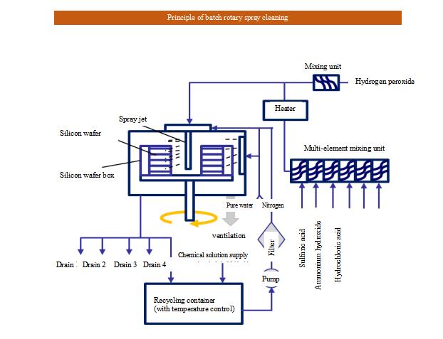
In the advanced process of integrated circuit manufacturing, single-wafer cleaning has gradually replaced wet bench cleaning as the mainstream choice. Firstly, single-wafer cleaning can provide better process control in the whole manufacturing cycle, improve the uniformity between a single wafer and different wafers, and improve the yield of products; secondly, larger wafers and more advanced process design are more sensitive to impurities, and the cross-contamination effect of wet bench cleaning will be greater, thus endangering the yield of the whole batch of wafers and incurring high expenses on core rework. In addition, the introduction of single-wafer & tank combined cleaning technology can integrate the advantages of single-wafer cleaning and wet bench cleaning, improve cleaning capacity and efficiency, reduce the use of sulfuric acid, help customers reduce costs, and meet the national policy requirements of energy conservation and emission reduction.
C. Situation of the semiconductor cleaning equipment industry
In recent years, the development of chip manufacturing technology has been the driving force of the development of semiconductor cleaning equipment. With the continuous development of chip process, the frequency of cleaning process needs to be greatly increased, and the number of cleaning equipment required will continue to grow, which brings huge new market demand for cleaning equipment. In addition, in order to further improve the performance of integrated circuits, the chip structure begins to transform towards 3D. At this time, on the basis of cleaning the wafer surface, the cleaning equipment also needs to clean internal pollutants without damage. This brings higher technical requirements for cleaning equipment. Advances in chip technology and the complexity of chip structures have led to the continuous increase in the value of cleaning equipment.
According to Gartner’s statistics, the global semiconductor cleaning equipment market size was USD 3.417 billion in 2018. In 2019 and 2020, as affected by the downturn in the global semiconductor industry, it was reduced by USD 3.049 billion and USD 2.539 billion, respectively. As the global semiconductor industry recovers in 2021, the global semiconductor cleaning equipment market will grow year by year, and the global semiconductor cleaning equipment industry is expected to reach USD 3.193 billion in 2024. According to Gartner’s statistics and forecasts, the global semiconductor cleaning equipment industry from 2018 to 2024 is as follows:
2018-2024 global semiconductor cleaning equipment market (USD 100mn)
Data source: Gartner
D. The global semiconductor cleaning equipment market is highly concentrated
In the global cleaning equipment market, Japanese companies are dominant, with DNS occupying a market share of over 40%; TEL, LAM, etc. also have large market shares, so the degree of market concentration is high.
E. Despite the rapid growth of semiconductor cleaning equipment enterprises in mainland China, the localization rate is still not high
At present, Chinese mainland’s leading cleaning equipment manufacturers are ACMSH, NAURA, KINGSEMI, and PNC, with different focus areas. Among them, the main products of ACMSH are single-wafer cleaning equipment in the field of integrated circuits, including single-wafer SAPS megasonic cleaning equipment, single-wafer TEBO megasonic cleaning equipment, single-wafer back cleaning equipment, single-wafer front scrubbing equipment, wet bench cleaning equipment and single-wafer & chamber combined cleaning equipment, etc., with a very rich product line. As for NAURA, after it acquired US semiconductor equipment manufacturer Akrion Systems LLC, its main products are single-wafer and wet bench cleaning equipment. KINGSEMI’s products are currently mainly used in the single-wafer cleaning in the integrated circuit manufacturing field. PNC has the relevant technology
to produce 8-12 inch high-end single-wafer wet cleaning equipment and trough wet cleaning equipment, which can cover the market demand for many downstream industries including wafer manufacturing, advanced packaging, and solar energy. Amid the wave of semiconductor factory construction in mainland China, investment in the Chinese semiconductor industry has been soaring. Chinese mainland semiconductor equipment manufacturers have made technological breakthroughs, and have entered the mainstream production lines of wafer manufacturers at home and abroad in the field of cleaning equipment. According to the Strategies for the Semiconductor Equipment Industry for 2020 issued by BOCI Securities in December 2019, domestic cleaning equipment has occupied over 20% of the Chinese mainland market, and the market share of China’s semiconductor cleaning.
| ② | Semiconductor electroplating equipment |
A. Semiconductor electroplating and electroplating equipment
Semiconductor electroplating refers to the electroplating of metal ions in the plating solution onto the wafer surface to form metal interconnection during the chip manufacturing process. With the chip manufacturing technology becoming more and more advanced, the interconnection wires in the chip begin to change from the traditional aluminum materials to copper materials, and semiconductor copper plating equipment is widely used. At present, the semiconductor electroplating is not limited to the deposition of copper wires; there are tin, tin silver alloy, nickel and other metals, but the deposition of copper is still dominant. Copper conductor can reduce the interconnection impedance, reduce the power consumption and cost of the device, and improve the speed, integration, device density, etc. of the chip.
The semiconductor electroplating equipment deposits a layer of copper on the silicon wafer, which is dense, free of holes, gaps and other defects, and evenly distributed. Then, it is coupled with vapor deposition equipment, etching equipment, cleaning equipment, etc. to complete the copper interconnection process.
Diagram on the front-end copper interconnect electroplating process in the chip manufacturing
In semiconductor electroplating, with the development of wafer-level packaging technology, the deposition process of metallized film is needed in three-dimensional silicon through-holes, rewiring and bumping process. The electroplating process is used to deposit copper, nickel, tin, silver, gold and other metals.
Diagram for the ee back-end advanced packaging electroplating process in chip manufacturing
B. Situation of the semiconductor electroplating equipment market
The field of electroplating equipment for front-end wafer manufacturing is currently dominated by LAM worldwide. Besides LAM, ACMSH is one of the few companies around the world that have mastered the core patent of copper plating technology for chip interconnection. It has independently developed the Ultra ECP map technology, a copper interconnection plating technology for front-end chip manufacturing for 20-14nm and more advanced technology nodes, and a new current control method of multi-anode local plating technology is used to realize fast switching (millisecond-level) between different anodes, and the hole-free filling is completed on the ultra-thin seed crystal layer; at the same time, by adjusting the current of different anodes, it ensures that the evenness of deposited copper film thickness is better after the hole-free filling. At present, ACMSH has received semiconductor electroplating equipment orders from customers on a continuous basis.
In the field of back-end advanced packaging and electroplating equipment, major equipment manufacturers in the world include Applied Materials and LAM (US), EBARA Corporation (Japan), ASM Pacific Technology Limited (Singapore), etc.; in domestic enterprises, ACMSH carried out differentiated development for advanced packaging process, and solved the problem of achieving stable electroplating under a larger flow of electroplating solution. Through its unique second-anode control technology, the film thickness uniformity control of the wafer flat edge or notch area can be better achieved at the process recipe level, and the yield of the packaging process is improved.
According to Gartner’s statistics, the global semiconductor electroplating market in 2018-2024 is as follows:
2018-2024 global semiconductor electroplating market (USD 100mn)
Data source: Gartner
| ③ | Advanced packaging equipment |
A. Introduction to advanced packaging and equipment
Semiconductor packaging is to connect the circuit pins on the wafer with wires to the external connector to facilitate connection with other devices. It plays a role in fixing, sealing, and protecting the chip and enhancing the electric heating performance, as well as in the connection between the internal chip and the external circuit.
Advanced packaging refers to the more advanced packaging form and technology at that time. At present, packages with flip chip (FC) structure, wafer level packages (WLP), 2.5D packages, 3D packages, fan-out packages, etc. are considered as advanced packages. The functions of advanced packaging include chip support and mechanical protection, electrical signal interconnection and extraction, power distribution and thermal management. According to the process of semiconductor packaging, semiconductor packaging equipment mainly includes wet etching equipment, wafer scrubbing equipment, film lamination equipment, developing equipment, film stripping equipment, thinning equipment, cutting equipment, electroplating equipment, cutting forming equipment, etc.
a. Wet etching equipment
Wet etching is a very important step in the semiconductor advanced packaging manufacturing process, and it is a main process of graphic processing associated with photolithography. Wet etching mainly uses the chemical reaction between the solution and the pre-etching materials to remove the part unshielded by the shielding film material. The wet etching equipment is the main equipment used in the wet etching process. Its working principle is as follows:
b. Film lamination/developing equipment
In the advanced semiconductor packaging process, the input (photoresist coating before exposure) and output (graphics development after exposure) of the photolithography equipment and the film lamination/developing equipment are mainly through transfers and processes of the wafer among various systems with a robot arm, thus completing the process of photoresist coating, curing, developing, film firming and other processes of the wafer, affecting the formation of fine exposure patterns in the photolithography process.
c. Film stripping equipment
In the advanced semiconductor packaging process, the film stripping equipment is used to remove the photoresist on the wafer surface as a barrier layer after the wafer is etched to avoid the residual photoresist from affecting the quality of subsequent processes. Its working principle is as follows:
d. Stress-free polishing equipment
In the advanced semiconductor packaging process, the stress-free polishing process is an innovative solution, which integrates stress-free polishing, chemical mechanical grinding and wet etching processes. Before the chemical mechanical grinding and wet etching processes, the electrochemical method is used to remove the copper layer on the wafer surface without stress and release the stress of the wafer. It can significantly reduce the use of chemicals and consumables, protect the environment while reducing equipment costs. The equipment is mainly applied to 3DTSV, 2.5D silicon intermediate layer, RDL, HD fan-out packaging, etc. Its working principle is as follows:
B. Situation of the advanced packaging market
Semiconductor advanced packaging is a back-end link in the chip manufacturing process. Its market demand is closely related to the demand for downstream chip applications. In the background of the continuous growth of consumer electronics, IoT, 5G, and other product demand, the market demand of semiconductor advanced packaging is expected to continue its sustained rapid growth.
The global packaging & testing technology is undergoing transformation from traditional packaging to advanced packaging (FC, WLC, fan-out, etc.). According to Yole’s statistics, in 2017, the global advanced packaging output value exceeded USD 20 billion, accounting for about 38% of the global total output value. It is estimated that by 2020, it will exceed USD 30 billion, accounting for 44%. From the perspective of the growth rate of advanced packaging, from 2017 to 2023, the revenue of the entire semiconductor packaging market will grow at a compound growth rate of 5.2%, in which the growth rate of the advanced packaging market will be 7%, while that of the traditional packaging market will be 3.3%.9
According to Gartner’s statistics, the global advanced packaging equipment market demands and predictions are as follows:
Data source: Gartner
9 Data source: 2019 Research Report on Shanghai’s Integrated Circuit Industry Development, Economic and Information Technology Commission of Shanghai, Shanghai Integrated Circuit Industry Association
(IV) Issuer’s Technological Level, Characteristics, Sci-Tech Achievements, and Deep Integration with the Industry
Through continuous R&D investment and long-term technology and process accumulation, the Company has accomplished a series of scientific and technological achievements in new product development and production process improvement, which plays a key role in continuously improving product quality and enriching product layout. The scientific and technological achievements of the Company are an important part of the Company’s competitiveness, and also the basis for the sustainable growth of the Company’s product sales scale.
In 2017, 2018 and 2019, the Company’s sales revenue was RMB 253.5873 million Yuan, RMB 550.2691 million Yuan, and RMB 756.733 million Yuan, respectively, showing a continuous growth trend. The large-scale sale of the Company’s products is a concrete indication of the deep integration of the Company’s scientific and technological achievements with the industry. The Company’s main products are semiconductor cleaning equipment, semiconductor electroplating equipment and advanced packaging wet equipment, covering wafer manufacturing, advanced packaging and other fields.
Application of the Company’s products in front-end wafer manufacturing processes of IC manufacturing
Application of the Company’s products in back-end advanced packaging processes of IC manufacturing
| | 1. | Semiconductor cleaning equipment |
Semiconductor cleaning equipment is the core product of the Company, accounting for 86.27%, 92.91%, and 84.10%, respectively, of the Company’s main business revenue in the report period.
| (1) | Single-wafer cleaning equipment |
The Company has independently developed the SAPS and TEBO megasonic cleaning technology with global intellectual property rights protection, which solves the global problem of the uniform distribution of megasonic energy on the wafer and realizes the damage-free megasonic cleaning of graphic structures when the megasonic technology is applied to the integrated circuit monolithic cleaning equipment. In order to maximize productivity, the Company’s single-wafer cleaning equipment can be configured with multiple process chambers according to the customer’s needs, up to 18 chambers can be configured in a single unit, which can effectively improve the production efficiency of customers.
| ① | SAPS megasonic cleaning equipment is mainly used to clean flat wafer surfaces and high-aspect-ratio throughhole internal structures |
The distance between the wafer surface megasonic energy and the wafer and the megasonic generator changes periodically. In traditional megasonic cleaning process, the distance from different points on the wafer to the megasonic generator is different because of the warpage of the wafer caused by the stress following different processes. Therefore, the megasonic energy at different positions on the wafer is also different. It is impossible to achieve the even distribution of the megasonic energy on the wafer surface. Moreover, because of the error of hardware position control, the distribution of megasonic energy on the wafer surface is not uniform.
The SAPS megasonic technology independently developed by the Company adopts a sector megasonic generator. By accurately matching the wafer rotation speed, liquid film thickness, the location of the megasonic generator, alternative displacement and energy and other key process parameters, this technology controls the relative motion of the half wavelength range between the megasonic generator and the wafer in the process, so that the megasonic energy received at each point on the wafer within the process time is the same. In this way, the uniform distribution of the megasonic energy on the wafer surface is under good control.
In order to meet the increasingly stringent requirements of the semiconductor industry, based on the megasonic cleaning technology, the Company brought in the hydrogen function water process, in which it mixes extremely diluted cleaning agents of hydrogen, ppm orders of magnitude of nitrogen and other special gas in deionized water. The process is supplemented by megasonic, and it performs well in the removal of small particles. This minimizes environmental pollution and material loss.
SAPS megasonic cleaning equipment not only provides good effects on removing small particles, but also has a certain technical advantage on deep-hole cleaning with a high aspect ratio. When the deep hole of a wafer surface has a high aspect ratio, especially in the cleaning of TSV structure, the material exchange of cleaning chemical compositions in the groove can only be determined by diffusion. When the depth of the deep hole is large, the diffusion path becomes very long and the cleaning efficiency becomes lower and lower. In the traditional cleaning process, the thickness of the cleaning fluid boundary layer on the wafer surface is relatively large, and the liquid movement on the surface cannot affect the interior of the deep hole, thus forming convection. Under the megasonic action, the thickness of the boundary layer on the wafer surface becomes very thin. The liquid can enter into the deep hole by convection and cavitation vibration, creating the effect of agitation, which then accelerates the exchange of cleaning chemical compositions and improves cleaning efficiency.
The SAPS technology can improve the cleaning effect and better eliminate residuals and other random defects in the interconnection structure during chip manufacturing:
After contact/through-hole etching: the wet etching process is usually used to create patterns with high contact and through-hole density. After the etching process, the SAPS technology can be used to eliminate the random defects that may cause electric short circuit.
Before the deposition of barrier layer metal: for copper wiring, a metal diffusion barrier layer should be set at the top of the through-hole to prevent electricity leakage; before the deposition of barrier layer metal, the SAPS technology can be used to
eliminate the residual copper oxide to prevent poor adhesion between the residual copper oxide and the barrier layer, which could damage the performance.
| ② | TEBO megasonic equipment is mainly applied to the cleaning of graphic wafers, including advanced 3D wafer structures |
With the further reduction of the chip technology node and the further increase of the aspect ratio, the difficulty in cleaning graphic wafers has increased. After the chip technology node is further extended to below 50nm, and the graphics structure is developed to multi-layer 3D, the traditional megasonic cleaning technology can hardly control the steady-state cavitation effect of bubbles, resulting in bubble breakage, which then causes high-energy microjet damage to the graphics structure on the wafer surface.
The TEBO cleaning equipment independently developed by the Company is applicable to the cleaning of graphic wafers of 28nm and below. Through a series of rapid (frequency up to one million times per second) pressure changes, the bubble maintains its size and shape oscillation under the controlled temperature. In this way, the bubble is controlled in a stable shaking state without implosion, thus preventing the wafer microstructure from being damaged while enabling cleaning of the graphic structure of the wafer surface without damage. During the technical transition of device structures from 2D to 3D, the TEBO cleaning equipment of the Company can be applied to FinFET, DRAM, emerging 3D NAND and other more sophisticated products with 3D structures, as well as new nano devices and quantum devices in the future. It plays an increasingly important role in improving the product yield of customers.
The TEBO technology can be used in multiple steps to achieve effective, non-destructive cleaning:
A. Memory chip: in the process of manufacturing DRAM chips, the TEBO technology can be applied to up to 50 steps.
B. Logic chip: in the manufacturing process of a logic chip with the FinFET structure, the TEBO technology can be applied to 15 or more cleaning steps.
| (2) | Single-wafer & tank combined cleaning equipment |
With the continuous improvement of the advanced degree of the chip manufacturing process, tank cleaning equipment can no longer meet the technical requirements of 28nm and below, and the cleaning technology gradually changes from tank cleaning to single-wafer cleaning. This change greatly increases the consumption of sulfuric acid, which causes a series of safety problems and environmental issues.
The Tahoe cleaning equipment independently developed by the Company with global intellectual property protection integrates two modules in a single wet cleaning device: tank module and single-wafer module. In the tank module, it is equipped with sulfuric acid hydrogen peroxide mixture (SPM) cleaning and quick dump rinsing (QDR), and the SPM process solution is recycled in the independent tank module; after the tank cleaning, the wafer will be transferred to the single-wafer module in the wet state for further single-wafer cleaning processes; the single-wafer cleaning chamber can be flexibly configured according to the customer’s needs, such as the standard cleaning solution (SC-1), hydrofluoric acid (HF), ozone water (DI-O3), and other process solutions. The single-wafer cleaning chamber can be equipped with up to 4 swing arms, each of which can provide up to 3 process pharmaceutical solutions, and the system can also provide the IPA drying function required for graphic wafers. The Tahoe cleaning equipment can be used in dozens of key cleaning processes, such as photoresist removal, cleaning after etching, cleaning after ion implantation, cleaning after mechanical polishing, etc.
The cleaning effect and process applicability of Tahoe cleaning equipment can be comparable to that of single-wafer cleaning equipment. In addition, compared with single-wafer cleaning equipment, Tahoe cleaning equipment can significantly reduce the consumption of sulfuric acid, and help customers reduce the production cost and better comply with the Chinese government’s policy of energy conservation and environmental protection.
(3) Single-wafer back cleaning equipment
The back cleaning equipment is usually used for back film removal, polycrystalline silicon wet etching on the back of a wafer, wafer back thinning, and back metal pollution removal. With the decrease of chip thickness, the requirement of wafer back thinning becomes higher and higher. When the wafer thickness is less than 300μm, the traditional mechanical clamping method can easily cause wafer warping, deformation and even fracture. Besides, some processes require to protect the wafer front with nitrogen atmosphere during the wafer back process, in order to prevent the solution, steam, chemical contact, and mechanical scratches from damaging the wafer front.
The single-wafer back cleaning equipment developed by the Company adopts the Bernoulli chuck and applies the principle of aerodynamics suspension. After the wafer is fed into the cavity by the manipulator, the back of the wafer is facing up and the front of the wafer is facing down. In the process, high-purity nitrogen with precise flow control is continuously input into the gap between the wafer and the chuck through the gas pipeline beneath the chuck and the ring hole on the chuck surface. The equipment can be used for back metal pollution cleaning, back etching, and other core processes.
(4) Front-end scrubbing equipment
The single-wafer cavity is used to clean the front and back of the wafer according to specific processes. This equipment can perform processes such as wafer back cleaning, wafer edge cleaning, front-back double-fluid cleaning, etc.; the equipment covers a small area, has high production capacity and strong stability, and provides a variety of cleaning methods for flexible choices. It can be used in each cleaning process from the front-end stage to the back-end stage of the IC manufacturing process.
(5) Fully automatic tank cleaning equipment
The fully automatic tank cleaning equipment developed by the Company is widely applied in cleaning, etching, photoresist removal and other processes in the field of integrated circuit and advanced packaging. It uses pure water, alkaline solutions and acid solutions as cleaning agents, combined with spray, hot dip, overflow, bubbling, and other cleaning methods. It’s also paired with advanced IPA drying method, capable of cleaning 50 wafers at the same time. The equipment features a high degree of automation, good stability, high cleaning efficiency and low cross-contamination of metals, materials and particles. This equipment is mainly used in the cleaning process of 40 nm and above technical nodes.
| | 2. | Semiconductor electroplating equipment |
The electroplating equipment independently developed by the Company with international intellectual property protection has been verified by downstream customers and itselectroplating equipment for back-end advanced packagaing has entered the market and obtained repeated orders.
(1) Front-end copper interconnection copper electroplating equipment
The Company is currently one of the few companies in the world that have mastered the core patent of chip copper interconnection copper electroplating technology. The company has independently developed Ultra ECP map for IC front-end copper interconnection copper plating technology node for 28-14nm and below. The Company also provides the multi-anode local plating technology, which adopts a new current control method to realize the fast switching (millisecond-level) between different anodes, and the hole-free filling is completed on the ultra-thin seed crystal layer. At the same time, by adjusting the current of different anodes, it can achieve better uniformity of deposited copper film thickness after the hole-free filling.
(2) Back-end advanced packaging electroplating equipment
The Company has carried out differentiated development in the field of semiconductor advanced packaging, solved the problem of realizing stable electroplating under a larger flow of electroplating solution, and adopted its unique second-anode control technology to better control the high uniformity near wafer flat edges or notch areas, thus achieving better uniformity within the wafer and realizing electroplating under the condition of high current density; all metrics of bumping
products meet customers’ requirements. In the field of electroplating for high-density packaging, it can realize the electroplating of 2um ultra-fine RDL lines and various metal layers including copper, nickel, tin, silver and gold. The patented sealing technology of rubber ring sealing independently developed by the Company can achieve better sealing effects and prevent leakage of plating solution and overplating.
| | 3. | Semiconductor copper polishing equipment |
(1) Front-end copper interconnection copper polishing equipment
With the continuous improvement of the advanced degree of chip manufacturing process, the size of the metal Cu wiring inside the chip, as a conductive connecting device, is becoming smaller and smaller. At present, the Damascene process is mainly used for inter-layer wiring inside the chip. Chemical Mechanical Polishing (CMP) technology is used to grind and remove the Cu layer on the surface of each layer after wiring, leaving the copper in the dielectric layer as the wire. CMP technology is widely used because of its high flatness and global flattening effect. However, in the CMP process, a certain amount of pressure is needed to act on the wafer, which can easily cause scratches on the wafer surface, or even the loss of copper wire at the graphic edges.
In order to resolve the defects brought by CMP technology, the company has put forward the concept of Stress Free Polish (SFP) technology for the first time in the world. By using the principle of electrochemical reaction, in the process of polishing the metal film on the wafer surface, the mechanical pressure in the polishing process is completely abandoned, thus eliminating the damage of the mechanical pressure on the metal wiring. The advantage of SFP stress-free electrochemical polishing is that it will not cause mechanical damage to the wafer surface, thus ensuring the quality of the final copper interconnections.
With the development of key dimensions of integrated circuits towards the technical nodes of 7nm and below, ruthenium is gradually replacing Ta/TaN as the barrier layer of copper wiring because of its good conductivity, low leakage rate, immiscibility with copper and good combination with copper. However, as ruthenium has very stable chemical properties, is not easy to oxidize, and has high hardness, the CMP process has a relatively low removal rate of ruthenium, and the stress generated in the mechanical polishing process will cause the micro copper wires to break and damage the surrounding dielectric materials. After research, the company found that the SFP process can be used for electrolytic oxidation of the ruthenium surface, and then DHF etching can be used to achieve a good removal effect of ruthenium metal layers without mechanical stress. This solves the problem of damage of micro copper wires and surrounding dielectric materials. This technology can be used in copper interconnection process for technical nodes under 5nm and 3nm. Meanwhile, because there is no mechanical stress, it is easier to integrate ultra-low k dielectric (k < 2) with copper wires, so as to improve the operation speed of the chip.
(2) Back-end advanced packaging stress-free copper polishing equipment
With regard to the flattening application of 3D TSV, 2.5D silicon intermediate layer, RDL, HD fan-out and other metal layers in advanced packaging, the Company has independently developed the stress-free polishing equipment with global intellectual property protection, which features stress-free process, recyclable chemicals, lower costs of consumables, environmental protection and emission reduction, etc..
| | 4. | Advanced packaging wet cleaning equipment |
The Company adheres to the strategy of differentiated competition, and based on the advanced technology of integrated circuit front-end wet cleaning equipment, it expands product application to the advanced packaging application field. Taking the typical process of bumping packaging as an example, the single-wafer wet process equipment involved in the whole process includes cleaning equipment, film lamination equipment, developing equipment, film stripping equipment, wet etching equipment, stress-free polishing equipment, etc.
At present, the Company’s products for the advanced packaging industry cover the entire range of single-wafer wet process equipment and have entered the production
lines of enterprises and scientific research institutes, such as JCET, Fujitsu, SMIC Long Power, Nepes, NCAP China, the Institute of Microelectronics (IME) of the Chinese Academy of Sciences (CAS), etc.
| ① | Advanced packaging cleaning equipment |
It is used in the process of 12-inch and 8-inch wafer incoming material cleaning, cleaning before plasma pretreatment, cleaning after UBM layer titanium wet etching, scaling powder cleaning after reflow, etc. In addition to the conventional rotary spray method, according to different customer needs, the Company has developed SAPS megasonic, double-fluid nano spray, brush scrubbing, high-pressure liquid spray, and other auxiliary cleaning methods.
| ② | Single-wafer film lamination equipment |
It can be applied to the film lamination process of positive and negative glue and thin thick glue of 12-inch and 8-inch wafers. The chamber self-cleaning function, invented by the Company with global intellectual property protection, replaces the traditional manual chamber removal and cleaning method, thus preventing damage to the equipment caused by the frequent manual removal of the sophisticated film lamination equipment, and the harm to the human body when cleaning the glue chamber. In the mean time, it also greatly improves the cleaning efficiency, reduces the maintenance cost, and improves the service life of the equipment.
| ③ | Single-wafer developing equipment |
The Company’s single-wafer developing equipment adopts a development mode that combines spray and puddle and is compatible with the development process of 12-inch and 8-inch wafers.
| ④ | Single-wafer & tank combined film stripping equipment |
The single-wafer & tank combined film stripping equipment, independently developed by the Company with intellectual property protection, is applied to the wet etching process of 12-inch and 8-inch wafers. The equipment combines tank film stripping with single-wafer film stripping, and the immersion process is completed in the tank to soften and remove most of the thick glue. The subsequent removal of residual glue, pollutants and particles is completed by single-wafer film stripping, which can make up for the shortage of capacity of single-wafer film stripping equipment.
| ⑤ | Single-wafer wet etching equipment |
It is used in wet etching of 12-inch and 8-inch wafers and UBM of copper, titanium, nickel, tin, gold and other metals. The single-wafer wet etching equipment integrates all the pharmaceutical solution, pure water and the gas pipeline used for drying in a complete process into a cavity, featuring small equipment area occupation, low consumption of chemicals and pure water, and high flexibility of process adjustment.
| | 5. | Vertical furnace tube equipment |
The vertical furnace is one of the key process equipment in the manufacturing process of integrated circuits. It can process wafers in batches. According to process pressure and application, it can be divided into two types: atmospheric pressure furnace and low pressure furnace. The atmospheric pressure furnace mainly completes thermal diffusion doping, thin film oxidation, and high temperature annealing; while the low pressure furnace mainly realizes the deposition process of different types of thin films on the wafer surface, mostly polysilicon, silicon nitride, silicon oxide and other thin films.
The vertical furnace tube equipment developed by the company is mainly composed of wafer transfer module, process cavity module, gas distribution module, temperature control module, exhaust gas processing module and software control module. It is designed and manufactured for different applications and process requirements. It tirst concentrated on LPCVD equipment, and then developed to oxidation furnace and diffusion furnace, and finally entered the application of ALD equipment.
(V) Market Positions of the Issuer’s Products or Services and Major Enterprises in the Industry
| | 1. | Market positions of the issuer’s products or services |
The global market of semiconductor cleaning equipment is highly concentrated, especially in the field of single-wafer cleaning equipment. The total market share of DNS, TEL, LAM and SEMES is over 90%, of which the DNS’s market share is the highest (> 40%).
At present, in mainland China, only a few enterprises can provide semiconductor cleaning equipment. They mainly include: ACMSH, NAURA, Kingsemi, and PNC. Among them, ACMSH is the leading enterprise in China’s semiconductor cleaning equipment industry. Its main products are monolithic cleaning equipment in the field of integrated circuits, including single-wafer SAPS megasonic cleaning equipment, single-wafer TEBO megasonic cleaning equipment, single-wafer back cleaning equipment, single-wafer scrubbing equipment, tank cleaning equipment, single-wafer & tank combined cleaning equipment, etc.. Its product line is relatively diverse. Main cleaning equipment products of NAURA are single-wafer and tank cleaning equipment, which can be applied to the chip manufacturing with 65nm and 28nm technology nodes; PNC has the relevant technology to produce 8-12 inch high-end single-wafer wet cleaning equipment and trough wet cleaning equipment, which can cover the market demand for many downstream industries including wafer manufacturing, advanced packaging, and solar energy. Kingsemi’s current products are used in the field of single-wafer cleaning in the integrated circuit manufacturing field.
In the 2018 rankings of the top 5 dedicated semiconductor equipment manufacturers in mainland China, ACMSH ranked 4th. The details are as follows:
| 2 | NAURA |
| 3 | CETC Electronics Equipment Group Co., Ltd. |
| 4 | ACMSH |
| 5 | Kingsemi |
Data source: 2019 Research Report on Shanghai’s Integrated Circuit Industry Development, Economic and Information Technology Commission of Shanghai, Shanghai Integrated Circuit Industry Association.
In addition, according to the equipment bidding results of Huahong Group Wuxi project, ACMSH won the bid for 5 pieces of cleaning equipment, accounting for 27% of the total, ranking first in the field of cleaning equipment, higher than international competitors.
According to the bidding results of Yangtze Memory 3D NAND production line (20,000 pieces/month), ACMSH won 15 pieces of cleaning equipment (all single-wafer cleaning equipment), ranking second only to DNS, which won 18 pieces, including 12 pieces of single-wafer cleaning equipment and 6 pieces of tank cleaning equipment; For single-wafer cleaning equipment, ACMSH won the most orders, accounting for 32.61%.10
According to the results of winning bids for equipment from Yangtze Memory and Huahong Group (Wuxi Project and Huali Phase II Project), among the more than 200 cleaning tools purchased in total, the suppliers are ranked in order of the number of successful bids: DNS, ACMSH, LAM, TEL, NAURA, Kingsemi, etc., the proportions are 48%, 20.5%, 20%, 6%, 1%, 0.5% in order. ACMSH ranks second in market share, slightly higher than LAM.11
11 Data source: Semiconductor Equipment Localization Topic Nine – Cleaning Equipment, BOC Securities, May 2020
| | 2. | Major enterprises in the industry |
At present, the major enterprises in the global dedicated semiconductor equipment industry are as follows:
| (1) | Overseas enterprises in the industry |
| ① | Applied Materials (Applied Materials, Inc.) |
Founded in 1967, the company is a world-leading manufacturer of dedicated semiconductor equipment. Headquartered in the United States, the company provides manufacturing equipment, services and software to semiconductor, display and related industries. Its main products in the semiconductor field are various manufacturing equipment for chip manufacturing, including epitaxy, ion implantation, oxidation and nitridation, rapid heat treatment, physical vapor deposition, chemical vapor deposition, chemical mechanical flattening, electrochemical deposition, atomic layer deposition, etching, measuring and inspection tools. Its business presence is mainly in the US, mainland China, South Korea, Taiwan (China), Japan, Southeast Asia and Europe.
| ② | ASML (ASML Holding N.V.) |
Founded in 1984 and headquartered in the Netherlands, the company is one of the world’s leading manufacturers of photolithography equipment in the semiconductor industry. Its EUV photolithography equipment is in a global monopoly position.
Founded in 1976 and headquartered in the United States, the company is a leading equipment supplier in the world, providing process control and yield management solutions for semiconductor, data storage, LED and other related nano electronic industries. Its main products are detection, testing and data analysis equipment used in wafer manufacturing, packaging, and testing fields.
| ④ | DNS (SCREEN Holdings Co., Ltd.) |
Founded in 1943, the company is a Japanese dedicated semiconductor equipment and LCD production equipment company with customers in Japan, South Korea and Taiwan (China). The main products of DNS are cleaning equipment, etching equipment, film lamination/developing equipment, etc., among which its cleaning equipment has a high market share in the semiconductor industry, accounting for more than 40% of the global semiconductor cleaning equipment market.
| ⑤ | TEL (TOKYO ELECTRON LTD.) |
Founded in 1963, the company is one of the world’s leading manufacturers of semiconductor manufacturing equipment and LCD manufacturing equipment. The company’s main products mainly include vapor deposition equipment, film lamination/developing equipment, heat treatment and film forming equipment, dry etching equipment, CVD, wet cleaning equipment, testing equipment and flat LCD display equipment.
| ⑥ | LAM (LAM RESEARCH CORPORATION) |
Founded in 1980 and headquartered in Fremont, California, the company is one of the major suppliers of wafer manufacturing equipment and services to the global semiconductor industry. The company’s main products include etching equipment, vapor deposition equipment, electroplating equipment, cleaning equipment and other semiconductor processing equipment for manufacturing integrated circuits.
(2) Domestic enterprises in the industry
| ① | AMEC (Advanced Micro-Fabrication Equipment Inc. China) |
Founded in 2004, the company is a high-end semiconductor micro-processing equipment company based in China and oriented towards the whole world. It is a leading enterprise in China’s integrated circuit equipment industry. AMEC focuses on the R&D, production and sale of plasma etching equipment, deep silicon etching equipment, MOCVD equipment and other key equipment used in micro device fields such as integrated circuits, LED chips, etc. It got listed on the STAR Market of
Shanghai Stock Exchange in July 2019, and its operating income was RMB 1.947 billion Yuan in 2019.
| ② | NAURA (NAURA Technology Group Co.,Ltd.) |
Founded in 2001, the company was formed through strategic restructuring between Beijing Sevenstar Electronics Co.,Ltd. and Beijing North Microelectronics Co., Ltd. in 2016. Headquartered in Beijing, the company is engaged in the R&D, production, sale and technical services of basic electronic products. Its main products are dedicated semiconductor equipment, such as etching equipment, PVD equipment, vertical tempering furnace equipment and cleaning equipment, vacuum equipment, new-energy lithium battery equipment and precision components, as well as solutions for semiconductors, new energies, new materials and other fields. It got listed in Shenzhen Stock Exchange in March 2010, and its operating income was RMB 4.058 billion Yuan in 2019.
| ③ | Kingsemi (Shenyang XinYuan Microelectronic Equipment Co., Ltd.) |
Founded in 2002, the company is mainly engaged in the R&D, production and sale of dedicated semiconductor equipment. Its products include photoresist film lamination development equipment (film lamination/developing equipment and glue spraying equipment) and single-wafer wet process equipment (cleaning equipment, film stripping equipment, and wet etching equipment), which can be used for single-wafer processing of 6-inch wafers and below (for example, during LED wafer manufacturing) and 8/12-inch wafers (for example, for wafer manufacturing and advanced packaging). It got listed on the STAR Market of Shanghai Stock Exchange in December 2019, and its operating income was RMB 213 million Yuan in 2019.
| ④ | Changchuan Technology (Hangzhou Changchuan Technology Co., Ltd) |
Founded in 2008, the company is a high-tech enterprise committed to improving the technical level of China’s dedicated IC equipment and actively promoting the upgrade of the IC equipment industry. Since its establishment, Changchuan Technology has been focused on independent R&D and innovation of integrated circuit testing equipment. Its main products include testing equipment and sorting equipment. It got listed on the GEM of Shenzhen Stock Exchange in April 2017, and its operating income was RMB 399 million Yuan in 2019.
| ⑤ | PNC (Shanghai PNC Process Systems Co., Ltd.) |
Founded in 2000 and headquartered in Shanghai, the company mainly provides high-end advanced manufacturing enterprises with high-purity process system solutions. Its main products include various system integration solutions, high-purity gas supply equipment, high-purity chemical transportation and distribution equipment, wet process equipment, ultra clean electronic materials, high-purity media special testing services, biopharmaceutical systems and equipment, etc. It got listed on the Shanghai Stock Exchange in January 2017.
(VI) Issuer’s Competitive Advantages and Disadvantages
(1) Technological advantage
Since its founding, the Company has adhered to the development strategy of differentiated competition and innovation, established a relatively sound intellectual property system through independent R&D, and formed a product line at the internationally leading or advanced level in semiconductor cleaning equipment, semiconductor electroplating equipment, advanced packaging wet-process equipment, stress-free polishing equipment, vertical furnace tube equipment and other product lines by virtue of rich technology and process accumulation. It is committed to providing advanced equipment and process solutions for global IC manufacturing industry.
The Company mainly adopts the mode of independent R&D. The R&D department is guided by the international technical trends and customer demands of dedicated semiconductor equipment and adopts the strategy of differentiated competition. In the R&D process, relying on the Company’s R&D team with rich
experience both home and abroad, the Company develops new processes and technologies, completes the verification of technical solutions, and applies for patent protection in major semiconductor production countries and regions to rapidly industrialize its R&D achievements.
The Company’s core technologies, such as SAPS and TEBO megasonic cleaning, single-wafer & tank combined cleaning, advanced electroplating, stress-free polishing, etc. are independently developed and have built intellectual property protection. SAPS and TEBO cleaning equipment products of the Company have solved, for the first time ever in the world, two major global problems in the application of megasonic cleaning technology in single-wafer cleaning equipment: the problem of uneven distribution of surface megasonic energy caused by wafer warpage and the problem of chip structure damage caused by megasonic cavitation breakage on the surface of graphic wafers. SAPS technology of the Company has been successfully applied to the manufacturing of DRAM, 3D NAND and logic circuit chips to help customers improve product yield effectively. Meanwhile, SAPS technology is also used for final cleaning after polishing of the semiconductor silicon wafer. The equipment has entered many 8-inch and 12-inch semiconductor silicon wafer manufacturers in mainland China and Taiwan (China). TEBO technology has been preliminarily verified in the logic chip factory. It can realize non-destructive cleaning on graphic chips, and its performance is especially remarkable in the cleaning efficiency of small particles.
The Company has launched the Tahoe single-wafer & tank combined cleaning equipment with global intellectual property rights protection, as the first one in the world. The equipment has been preliminarily verified by large domestic clients. It can greatly save sulfuric acid consumption compared with the existing single-wafer cleaning equipment. In the next few years, it will solve the global semiconductor chip industry problems that have plagued integrated circuit manufacturers for many years, such as large sulfuric acid consumption and difficult processing.
In the field of semiconductor electroplating equipment, in 2018, the Company’s advanced packaging and electroplating equipment entered the market. This equipment adopts the Company’s unique patented technology to solve the uniformity problem of the plating film of wafer flat edges or notched area. With its technical innovation, it has broken up the market monopoly of global giants. In 2019, the first front-end copper interconnection electroplating equipment successfully entered the client. The equipment adopts the core technology of multi-anode local copper electroplating, independently developed by the Company with global intellectual property protection, which can realize uniform plating on ultra-thin seed crystal layers and greatly improve the process window of cavitation-free plating in small holes.
The stress-free copper polishing and chemical mechanical polishing (CMP) integrated equipment, independently developed by the Company with global intellectual property protection, also entered the advanced packaging client in 2019 for process testing. The equipment adopts the patented technology of stress-free electropolishing independently developed by the Company. It can greatly save the cost of polishing process consumables, compared with the traditional CMP equipment. The Company will apply the stress-free polishing technology to the copper interconnection process under the technical nodes of 5nm and 3nm. At the same time, because there is no mechanical stress, it is easier to integrate the ultra-low k dielectric (k < 2) with the copper wires, so as to improve the operation speed of the chip.
The Company has also developed a series of wet process equipment for advanced packaging, including scrubbing, wet etching, film lamination, developing, film stripping equipment, etc. These devices have successfully entered the main production lines of domestic advanced packaging clients, and combined with copper plating and stress-free polishing equipment, they can provide a complete set of wet process equipment and solutions for advanced packaging clients.
The company’s technical level for the megasonic single-chip cleaning equipment, single-chip slot-type combined cleaning equipment and electroplating process equipment of copper interconnection, has reached international leading or international advanced level. As of December 31, 2019, the company and its holding subsidiaries has 232 main licensed patents, including 108 domestic patents and 124 overseas patents.
Among them, there are 227 invention patents. The company also won the title of “Shanghai Key Laboratory of Advanced Wet Process Equipment for Integrated Circuits”. It is the main subject unit of major scientific research projects in China such as “Research and development and application for 20-14nm copper plating equipment of copper interconnection” and “Research and development for 65-45nm stress-free polishing equipment of copper interconnection”, and other (“02 Special Project”) major scientific projects in China.
Through continuous R&D investment and technology and process accumulation, the Company boasts certain technological advantages in industrial competition with its development strategy of differentiated competition and innovation.
(2) Technical R&D team advantage
The Company attaches great importance to the development and training of its technology R&D team, and encourages independent innovation and independent R&D. Since its founding, the Company has continuously trained and brought in professional talents in the global industry. After years of accumulation, the Company now has an international professional technology R&D team. Dr. Hui Wang is the core leader of this core R&D team. Most of the main R&D personnel have overseas study or practice experience, with global vision and thinking, which is conducive to learning and mastering international advanced technologies. In addition, the company has established a professional R&D team in South Korea, and by relying on South Korea’s technical personnel in the field of mechanical and electronic, such team and the Mainland China’s R&D team learn from each other. By establishing an international and professional technical R&D team and adhering to differentiated technological innovation and competitive strategies, the Company ensures that it can continuously launch new products and continuously improve existing products to consolidate and enhance the Company’s technological research and development capabilities. As of December 31, 2019, the Company has 150 technical R&D personnel, accounting for 41.90% of the Company’s employees. During the reporting period, the Company’s core technology R&D team is stable and has a strong team advantage in technical R&D.
(3) Customer verification advantage
Integrated circuit manufacturing enterprises have strict requirements for the technical standards and reliability of all kinds of equipment, and they are very cautious in the selection of equipment suppliers. Usually, integrated circuit manufacturers will require equipment suppliers to provide equipment product for testing, and only after passing the internal verification (some need to obtain the verification of their downstream customers), can they formally sign a purchase contract, and once the equipment is verified and actually entered the production line, it will become the first choice for customers to build the next production line, and will not be easily replaced. After years of efforts, by virtue of our technical and service advantages in the field of cleaning equipment and semiconductor electroplating equipment, some equipment having passed the verification, and the Company has become the certified supplier of well-known semiconductor companies in the industry, such as Hynix, Yangtze Memory, Huahong group, SMIC, etc., and entered multiple production lines of these customers, achieved good market reputation, and established a good trust relationship with these customers. Through the cooperation with the above-mentioned integrated circuit manufacturing enterprises, the Company has a deeper understanding of customers’ core needs and technical trends, which helps the Company get closer to customers’ needs when choosing the R&D directions. Therefore, the Company currently has certain advantages in customer verification.
(4) Global procurement system advantage
As a company specializing in semiconductor equipment that faces the forefront of international technology and insisting on independent innovation, the Company is mainly engaged in technology and process R&D, design of equipment product, and providing equipment and process solutions to customers, with no engagement in parts processing business through following the global industry practice. Considering the precision of the semiconductor special equipment, the Company has strict requirements on the quality of raw materials and components. High-precision, high-quality, high-reliability raw materials and components are important guarantees for the Company’s equipment performance and stability.
The Company has established a global procurement system and a stable cooperative relationship with major suppliers. The Company has established ACM South Korea and ACM California branches to build a procurement team for raw materials and components. Relying on the relatively developed and sound semiconductor industry chains in these two countries, the Company finishes procurement of some key components overseas. At the same time, the Company actively cooperates with local raw material and parts suppliers in mainland China, While gradually improving the diversification of procurement channels for key parts, such efforts can also shorten the procurement cycle of raw materials and parts and reduce the procurement cost.
(5) Operation cost advantage
In the field of semiconductor cleaning equipment, the Company’s main competitors are in the United States and Japan, where the R&D and production staff costs are high, and the cost of serving customers in mainland China is rather high. The Company’s R&D and production are mainly located in mainland China, where the labor costs are relatively low. The Company has established a global procurement system and cultivated some suppliers in mainland China. Through close cooperation with suppliers in product design, the Company’s products are modular and easy to maintain, which reduces the Company’s raw material procurement costs. Compared with the Company’s main competitors, the Company has certain advantages in operating costs.
(6) Quick response advantage
The production bases of the Company’s main customers are all located in mainland China. Compared with its international competitors, the Company is closer to the main customers geographically and can provide faster and more economic technical support and customer maintenance. The Company has established a technical team and after-sales service team, made up of well-experienced veteran staff, in the production
bases of main customers. In this way, the Company can understand the needs of customers in real time, respond to customers’ requirements quickly, and troubleshoot and solve problems in time, so as to ensure the normal, stable and continuous operation of the Company’s equipment on the customers’ production lines. Compared with major competitors, the Company has the advantages in quick response.
(7) Location advantage
The Company’s main R&D and production base is located in Shanghai. Shanghai, as an important leading city of the integrated circuit industry in mainland China, has formed a complete integrated circuit industry chain which integrates design, manufacturing, packaging, measurement, materials, equipment and other supporting services. The city’s industrial structure is the most complete and most balanced in the domestic IC industry chain.
Besides, as an integrated circuit industry cluster area with early development and the most complete industry chain in China, Shanghai has established a relatively complete integrated circuit talent education and training system. There are many institutions of higher learning and scientific research institutes in Shanghai, which not only provide talents to integrated circuit enterprises, but also provide the basis for the combination of production, learning and research.
With Shanghai being an international financial center and a leading IC city, the Yangtze River Delta region, which centers around Shanghai, has gathered many leading enterprises from the integrated circuit industry chain, such as Hynix, HLMC, Huahong Group, SMIC, etc. In addition, the presence of many supporting industries such as machining, production accessories, electronic information, etc. also gives Shanghai’s dedicated semiconductor equipment enterprises obvious location advantages in terms of customer resources, supplier procurement, talent training and introduction, compared with domestic competitors.
(8) First mover advantage
ACMR, the controlling shareholder of the Company, was founded in Silicon Valley in 1998, the Company has been engaged in the R&D of special semiconductor equipment ever since. In 2005, ACMR invested in Shanghai to set up the Company’s predecessor, Shengmei Co., Ltd., and invested the right to use the technology for semiconductor special equipment formed by its previous R&D into Shengmei Co., Ltd., and continued to carry out continuous research and technology accumulation with the Company as the subject..
The Company was one of the earliest enterprises to enter the field of semiconductor cleaning equipment and semiconductor electroplating equipment in mainland China. When its domestic competitors appear, the Company has formed a series of core technologies with independent intellectual property rights through long-term R&D and technology accumulation, and effectively reduced costs through large-scale procurement and production. Therefore, the Company has formed a strong first-mover advantage in the competition with domestic enterprises, it has become a leading company in the field of semiconductor cleaning equipment, and has the technical strength to compete with international giants.
| | 2. | Competitive disadvantages |
(1) Its market reputation needs improving
In recent years, by virtue of stable and reliable quality and excellent after-sales service, the Company’s equipment has gradually entered the production lines of many domestic and foreign leading manufacturing enterprises, and has obtained a certain market share. With the Company’s continuous investment in R&D and market exploration, the Company has achieved a certain market reputation in the mainland China market. However, in the international market, international semiconductor special equipment giants have the advantages of long time to market, large scale, prominent market position and complete international layout. Compared with these international giants, the company still has certain disadvantages in market reputation.
(2) Its scale is small compared with that of international giants
Currently, the semiconductor professional equipment industry is highly concentrated. In 2018, the market share of the top five semiconductor special equipment companies in the world reached 71%, with a total sales of USD52.784 billion dollars. During the reporting period, the Company’s main business revenue was RMB 249.1381 million Yuan, RMB 539.6117 million Yuan, and RMB 743.4081 million Yuan, respectively. Despite the trend of sustained and rapid growth, the Company’s business scale is relatively small compared with that of global industry giants, and there are certain disadvantages in the bargaining power and risk resistance ability of raw material procurement.
(VII) Development Situation, Opportunities, and Challenges of the Industry
| | 1. | Development situation and opportunities of the industry |
(1) The market demand for semiconductor application and consumption will continue to grow for the long term
In recent years, with the rapid development of electronic information technology, all types of intelligent, networked and mobile portable consumer electronic products have emerged one after another, and new-generation network communication, IoT, cloud computing, energy conservation and environmental protection, and other emerging industries have become the new driving force for the development of the semiconductor industry, jointly promoting the sustained, rapid and vigorous development of the global semiconductor industry. With China becoming one of the most important production bases of electronic information products in the world, more and more international semiconductor enterprises are shifting production capacity to China. The continuous production capacity migration not only promotes the overall industrial scale and technical level of the domestic semiconductor industry, but also provides huge market space for the dedicated semiconductor equipment manufacturing industry, and promotes the cultivation of professional talents in mainland China’s semiconductor industry as well as supporting industries. The healthy development of the semiconductor industry provides opportunities for the expansion and upgrading of China’s dedicated semiconductor equipment manufacturing industry.
(2) Regional shift of the global semiconductor industry
The semiconductor industry involves many production technology processes, many product types, rapid technological upgrades, high investment risks, wide downstream applications, etc.. With the continuous emergence of downstream emerging application markets, the trend of the semiconductor industry chain transforming from integration to vertical division of labor is becoming clearer and clearer. At present, the global semiconductor industry is starting its third industrial migration, this time to Chinese mainland. In history, the first industrial shift to Japan and the second industrial shift to South Korea and China Taiwan have driven the development of local industries, the advancement of vertical division of labor and the optimization of resource allocation. For the target countries and regions of industrial migration, the local semiconductor industry tends to extend from packaging & testing to wafer manufacturing and chip design, to semiconductor materials and equipment, and ultimately to realization of the overall development of the entire industry chain. Compared with developed countries and regions, the division of labor in the semiconductor industry chain in mainland China is still in the early stage, and the dedicated semiconductor equipment industry will become the focus of future growth.
The accelerated shift of the semiconductor industry towards mainland China brings direct benefits to China, which is the largest semiconductor terminal consumer market in the world. The scale of China’s semiconductor industry is expanding. With the continuous shift of international capacity to China, semiconductor enterprises are investing in mainland China to build new plants. It is expected that the demand for dedicated semiconductor equipment in mainland China will continue to grow.
(1) Lack of high-end technology and talent
The dedicated semiconductor equipment industry is a typical technology-intensive industry, which has high requirements for the knowledge background, R&D ability and operation experience accumulation of technical personnel. As R&D in China began very late, the industry still lacks talents and technology, which restricts the rapid development of the industry to a certain extent.
(3) Weak supporting capacity for domestic core components
The overall scale of domestic dedicated semiconductor equipment is not large enough, the pulling time of the parts market is short, and the matching capacity of parts of dedicated semiconductor equipment is weak. Consequently, the manufacturing cost of dedicated semiconductor equipment is high.
III. Issuer’s Sales and Main Customers
(I) Output and Sales of Main Products
The Company designs its production process according to modularization. In the production process, the cavity, liquid supply system and electronic control module are pre-assembled before the whole equipment is assembled. The production process is relatively simple, and the pre-job training is fast. The Company can flexibly adjust the number of workers according to the actual order. Most parts of the Company’s products are mainly procured through outsourcing. The assembly and inspection cycle in the factory is short, and the production process occupies only small numbers of fixed assets.
All in all, the Company’s production capacity is flexible to a certain extent, and it can flexibly arrange manual production according to specific orders. Due to the fluctuation of the semiconductor industry demand, the investment expansion of downstream customers may be relatively concentrated, resulting in the sudden large order demand of equipment manufacturers. The Company’s short-term labor force and assembly and testing equipment will limit the Company’s production to a certain extent, and the short-term supply capacity of upstream suppliers’ raw materials will also limit the production in response to the sudden demand. These factors restrict the Company’s production capacity to some degree.
| | 1. | Output and sales of main products |
(1) Output and sales of main products
During the reporting period, the Company’s output and sales were as follows:
Unit: piece
| Product Category | Item | 2019 | 2018 | 2017 |
| Semiconductor cleaning equipment | Output | 28 | 22 | 11 |
| Sales | 26 | 21 | 11 |
| Output/sale ratio | 92.86% | 95.45% | 100.00% |
| Semiconductor electroplating equipment | Output | 4 | - | 1 |
| Sales | 4 | 1 | - |
| Output/sale ratio | 100.00% | - | - |
| Advanced packaging wet process equipment | Output | 9 | 13 | 7 |
| Sales | 7 | 6 | 7 |
| Output/sale ratio | 77.78% | 46.15% | 100.00% |
| | 2. | Sales revenue of main products |
During the reporting period, the revenue of the Company’s main business was as follows:
Unit: RMB 10,000 Yuan
| Item | 2019 | 2018 | 2017 |
| Amount | Proportion | Amount | Proportion | Amount | Proportion |
| Semiconductor cleaning equipment | 62,522.30 | 84.10% | 50,135.96 | 92.91% | 21,492.48 | 86.27% |
In which: single-wafer cleaning equipment | 55,099.52 | 74.12% | 50,135.96 | 92.91% | 21,492.48 | 86.27% |
Tank cleaning equipment | 4,801.36 | 6.46% | - | - | - | - |
Single-wafer & tank combined cleaning equipment | 2,621.43 | 3.53% | - | - | - | - |
| Semiconductor electroplating equipment | 7,857.39 | 10.57% | 1,191.13 | 2.21% | - | - |
| Advanced packaging wet process equipment | 3,961.12 | 5.33% | 2,634.07 | 4.88% | 3,421.33 | 13.73% |
| Total | 74,340.81 | 100.00% | 53,961.17 | 100.00% | 24,913.81 | 100.00% |
The Company’s main customers are as follows:
| SN | Customer’s Field | Customer Name |
| 1 | Wafer manufacturing | Hynix, Huahong Group, Yangtze Memory, SMIC, Hefei Innotron |
| 2 | Advanced packaging | JCET, Fujitsu, SMIC Long Power, Nepes |
| 3 | Semiconductor silicon wafer manufacturing and recycling | Shanghai ZINGSEMI, JRH, Taiwan Wafer Works Corporation, Taiwan Phoenix Silicon |
| 4 | Scientific research institutes | Institute of Microelectronics of the Chinese Academy of Sciences, Shanghai IC, NCAP China |
| | 3. | Overall changes in sales prices |
During the reporting period, the Company’s main products were all customized. According to the different needs of customers, the average sales price of the products varies as follows:
Unit: RMB 10,000 Yuan/piece
| Item | 2019 | 2018 | 2017 |
Average Price | Growth | Average Price | Growth | Average Price |
| Semiconductor cleaning equipment: | | | | | |
| Single-wafer cleaning equipment | 2,504.52 | 4.90% | 2,387.43 | 22.19% | 1,953.86 |
| Tank cleaning equipment | 1,600.45 | - | - | - | - |
| Single-wafer & tank combined cleaning equipment | 2,621.43 | - | - | - | - |
| Semiconductor electroplating equipment | 1,964.35 | 64.91% | 1,191.13 | - | - |
| Advanced packaging wet process equipment | 565.87 | 28.90% | 439.01 | -10.18% | 488.76 |
(II) Sales to Top Five Customers
During the reporting period, the Company’s sales to the top five customers were as follows:
Unit: RMB 10,000 Yuan
| 2019 |
| SN | Name | Amount | Proportion |
| 1 | Yangtze Memory | 21,888.34 | 28.92% |
| 2 | Huahong Group | 20,734.59 | 27.40% |
| 3 | Hynix | 15,193.35 | 20.08% |
| 4 | JCET | 5,620.56 | 7.43% |
| 5 | SMIC | 2,649.74 | 3.50% |
| Total | 66,086.58 | 87.33% |
| 2018 |
| SN | Name | Amount | Proportion |
| 1 | Huahong Group | 12,667.23 | 23.02% |
| 2 | Yangtze Memory | 12,653.88 | 23.00% |
| 3 | Hynix | 12,117.32 | 22.02% |
| 4 | Qianjing International | 6,935.04 | 12.60% |
| 5 | ACMR | 6,081.94 | 11.05% |
| Total | 50,455.41 | 91.69% |
2017
|
| SN | Name | Amount | Proportion |
| 1 | Qianjing International | 13,844.90 | 54.60% |
| 2 | Hynix | 6,784.03 | 26.75% |
| 3 | ACMR | 4,389.52 | 17.31% |
| 4 | HANWOOL | 183.01 | 0.72% |
| 5 | SMIC | 109.95 | 0.43% |
| Total | 25,311.40 | 99.81% |
Note: 1. Yangtze Memory includes Yangtze Memory Technologies Co., Ltd. and Wuhan Xinxin Semiconductor Manufacturing Co., Ltd. 2. Huahong Group includes Huahong Semiconductor (Wuxi) Co., Ltd., Shanghai Huahong Hongli Semiconductor Manufacturing Co., Ltd., Shanghai Huali IC Manufacturing Co., Ltd., Shanghai Huali Microelectronics Corporation, and Shanghai IC R&D Center. 3. Hynix includes SK Hynix Inc. and SK Hynix Semiconductor (China) Co., Ltd. 4. SMIC includes Semiconductor Manufacturing North China (Beijing) Corporation, SMIC IC Manufacturing (Shanghai) Co., Ltd., Semiconductor Manufacturing South China Corporation, and SMIC Long Power Semiconductor (Jiangyin) Co., Ltd.
During the reporting period, in 2017 and 2018, part of the Company’s export business was carried out through Qianjing International, an import and export service provider. Specifically, the Company first sold the products to Qianjing International, which subsequently went through the customs declaration formalities. Qianjing International sold the products to the final customers at the same price, and the Company paid the export customs declaration agency fee to Qianjing International. After June 2018, the Company’s export business was carried out through Hong Kong CleanChip, a wholly-owned subsidiary in Hong Kong. The Company no longer has business with Qianjing International.
In 2017 and 2018, some customers of the Company placed orders with ACMR, and the Company sold the products to ACMR, which then sold them to final customers. In 2019, the Company did not sell products to final customers through ACMR.
During the reporting period, the Company’s top 5 final customers were as follows:
Unit: RMB 10,000 Yuan
| 2019 |
| SN | Name | Amount | Proportion |
| 1 | Yangtze Memory | 21,888.34 | 28.92% |
| 2 | Huahong Group | 20,734.59 | 27.40% |
| 3 | Hynix | 15,193.35 | 20.08% |
| 4 | JCET | 5,620.56 | 7.43% |
| 5 | SMIC | 2,649.74 | 3.50% |
| Total | 66,086.58 | 87.33% |
| 2018 |
| SN | Name | Amount | Proportion |
| 1 | Yangtze Memory | 18,735.81 | 34.05% |
| 2 | Huahong Group | 15,314.19 | 27.83% |
| 3 | Hynix | 12,117.32 | 22.02% |
| 4 | JCET | 2,536.22 | 4.61% |
| 5 | SMIC | 2,188.16 | 3.98% |
| Total | 50,891.71 | 92.49% |
| 2017 |
| SN | Name | Amount | Proportion |
| 1 | Hynix | 6,784.03 | 26.75% |
| 2 | Huahong Group | 5,413.51 | 21.35% |
| 3 | SMIC | 5,097.38 | 20.10% |
| 4 | Yangtze Memory | 4,389.52 | 17.31% |
| 5 | JCET | 2,403.48 | 9.48% |
| Total | 24,087.92 | 94.99% |
Note: 1. Yangtze Memory includes Yangtze Memory Technologies Co., Ltd. and Wuhan Xinxin Semiconductor Manufacturing Co., Ltd. 2. Huahong Group includes Huahong Semiconductor (Wuxi) Co., Ltd., Shanghai Huahong Hongli Semiconductor Manufacturing Co., Ltd., Shanghai Huali IC Manufacturing Co., Ltd., Shanghai Huali Microelectronics Corporation, and Shanghai IC R&D Center. 3. Hynix includes SK Hynix Inc. and SK Hynix Semiconductor (China) Co., Ltd. 4. SMIC includes Semiconductor Manufacturing North China (Beijing) Corporation, SMIC IC Manufacturing (Shanghai) Co., Ltd., Semiconductor Manufacturing South China Corporation, and SMIC Long Power Semiconductor (Jiangyin) Co., Ltd.
During the reporting period, the total sales of the Company’s top five end customers accounted for 94.99%, 92.49% and 87.33% of the total sales of the current period respectively. The Company did not encounter situations where the proportion of sales to a single end customer exceeds 50% of the Company’s total sales in the current year or relies heavily on a few customers. Except ACMR and
Huahong Group’s subsidiary, Shanghai IC , during the reporting period, the Company has no relationship with the top five customers and the top five end customers.
IV. Issuer’s Procurement and Main Suppliers
(I) Issuer’s Procurement
| | 1. | Procurement of main raw materials |
(1) Procurement amounts of main raw materials
During the reporting period, the main raw materials procured by the Company included categories of gas circuit, material transport, machinery, electric components, etc. The composition of each category of raw materials is as follows:
| SN | Category | Content |
| 1 | Gas circuit | Valve, contact, filter, pump, flowmeter, gas control module pneumatic components, cylinder, sensor, etc. |
| 2 | Material transport | Robot arm, wafer transport platform, etc. |
| 3 | Machinery | Cavity parts, cavity cabinet, rack, etc. |
| 4 | Electric components | Electronic components, sensor, programmable control module, DC power supply, circuit breaker, etc. |
| 5 | Special apparatus | Heater, functional water, ozone generator, CO2 mixing generator, cooler, hydrogen generator, megasonic generator, etc. |
| 6 | Drives | Motor and driver, guide rail, etc. |
| 7 | Others | Software, trunking, chemicals, procurement fees, etc. |
During the reporting period, the procurement amounts of the Company’s main raw materials and the proportions in the total raw material procurement amount were as follows:
Unit: RMB 10,000 Yuan
| SN | Item | 2019 | 2018 | 2017 |
| Amount | Proportion | Amount | Proportion | Amount | Proportion |
| I. Gas circuit |
| 1 | Valve | 3,538.90 | 7.85% | 3,541.02 | 8.13% | 1,237.20 | 6.96% |
| 2 | Contact | 1,932.78 | 4.29% | 2,311.47 | 5.31% | 865.20 | 4.87% |
| 3 | Filter | 1,790.03 | 3.97% | 1,528.20 | 3.51% | 734.48 | 4.13% |
| 4 | Pump | 1,578.02 | 3.50% | 1,741.01 | 4.00% | 808.86 | 4.55% |
| 5 | Flowmeter | 1,366.91 | 3.03% | 1,429.32 | 3.28% | 530.36 | 2.99% |
| 6 | Others | 2,668.42 | 5.92% | 1,762.56 | 4.05% | 656.88 | 3.70% |
| Subtotal | 12,875.05 | 28.55% | 12,313.58 | 28.28% | 4,832.98 | 27.21% |
| II. Machinery |
| 1 | Cavity parts | 5,801.98 | 12.87% | 4,647.12 | 10.67% | 1,596.99 | 8.99% |
| 2 | Cavity cabinet | 2,306.51 | 5.12% | 1,902.72 | 4.37% | 681.95 | 3.84% |
| 3 | Rack | 1,356.39 | 3.01% | 923.24 | 2.12% | 321.76 | 1.81% |
| 4 | Others | 303.26 | 0.67% | 7.30 | 0.02% | 66.45 | 0.37% |
| Subtotal | 9,768.14 | 21.66% | 7,480.38 | 17.18% | 2,667.14 | 15.01% |
| III. Material transport |
| 1 | Robot arm | 7,280.47 | 16.15% | 5,951.56 | 13.67% | 2,557.46 | 14.40% |
| 2 | Others | 415.73 | 0.92% | 110.03 | 0.25% | 165.18 | 0.93% |
| Subtotal | 7,696.20 | 17.07% | 6,061.59 | 13.92% | 2,722.64 | 15.33% |
| IV. Electric components |
| 1 | Electronic parts and components | 2,089.10 | 4.63% | 660.90 | 1.52% | 230.80 | 1.30% |
| 2 | Sensor | 1,944.46 | 4.31% | 2,547.59 | 5.85% | 1,022.54 | 5.76% |
| 3 | Programmable control module | 1,179.77 | 2.62% | 2,465.20 | 5.66% | 808.06 | 4.55% |
| 4 | Others | 855.83 | 1.90% | 2,611.14 | 6.00% | 297.52 | 1.67% |
| Subtotal | 6,069.17 | 13.46% | 8,284.83 | 19.03% | 2,358.93 | 13.28% |
| V. Special apparatus |
| 1 | Heater | 2,086.26 | 4.63% | 1,097.89 | 2.52% | 627.65 | 3.53% |
| 2 | Functional water | 1,002.58 | 2.22% | 993.18 | 2.28% | 779.61 | 4.39% |
| 3 | Generator | 2,805.47 | 6.22% | 4,945.97 | 11.36% | 2,325.74 | 13.09% |
| 4 | Others | 578.93 | 1.28% | 212.74 | 0.49% | 355.73 | 2.00% |
| Subtotal | 6,473.24 | 14.36% | 7,249.78 | 16.65% | 4,088.73 | 23.02% |
| VI. Driver |
| 1 | Motor and driver | 977.53 | 2.17% | 497.65 | 1.14% | 487.77 | 2.75% |
| 2 | Others | 98.47 | 0.22% | 51.29 | 0.12% | 13.70 | 0.08% |
| Subtotal | 1,076.00 | 2.39% | 548.94 | 1.26% | 501.47 | 2.82% |
| VII. Others |
| Subtotal | 1,135.28 | 2.52% | 1,598.08 | 3.67% | 591.73 | 3.33% |
| Total | 45,093.08 | 100.00% | 43,537.19 | 100.00% | 17,763.63 | 100.00% |
(2) Procurement prices of main raw materials
Based on the different needs of customers, the Company carries out professional customization and purchase raw materials accordingly. There are many kinds and models of raw materials required by the Company, and the procurement unit prices are not comparable. During the reporting period, the price index changes of the procurement prices of some categories of main raw materials of the Company were as follows:
| Raw Material Category and Model | Price Index |
| 2019 | 2018 | 2017 |
| Robot arm (8-cavity) | 95.94 | 95.94 | 100.00 |
| Robot arm (12-cavity) | 95.79 | 95.79 | 100.00 |
| Valve (402-1231) | 100.00 | 100.00 | 100.00 |
| Valve (402-1210) | 100.00 | 100.00 | 100.00 |
| Contact (400-1048) | 103.02 | 102.89 | 100.00 |
| Contact (400-1449) | 102.99 | 102.65 | 100.00 |
| Electronic parts and components (413-1165) | 97.05 | 99.50 | 100.00 |
| Megasonic generator (319-1073) | 94.94 | 87.81 | 100.00 |
| Megasonic generator (319-1047) | 97.97 | 88.14 | 100.00 |
| Cavity parts (110-6519) | 93.69 | 96.28 | 100.00 |
| Cavity cabinet | 92.46 | 100.61 | 100.00 |
Note: It is assumed that the 2017 price index is set as 100, and the 2018 and 2019 price indexes are calculated based on the average purchase price in 2017.
| | 2. | Procurement of main energies and relevant price change tendencies |
The issuer consumes small amounts of water, electricity and other energies in the production and R & D process. All the water and electricity are from the local water supply and power grid, and the supply is stable. The specific situation of the issuer’s water and electricity consumption during the reporting period is as follows:
| Energy | Item | 2019 | 2018 | 2017 |
| Water | Amount (RMB 10,000 Yuan) | 17.16 | 10.78 | 3.96 |
| Unit price (RMB Yuan/ton) | 4.95 | 4.92 | 4.87 |
| Electricity | Amount (RMB 10,000) | 161.91 | 150.15 | 121.79 |
| Unit price (RMB Yuan/kWh) | 1.02 | 1.03 | 1.00 |
(II) Procurement from Top 5 Suppliers
During the reporting period, the amounts and proportions of the Company’s procurement from the top 5 suppliers were as follows:
Unit: RMB 10,000 Yuan
| 2019 |
| SN | Name | Amount | Proportion | Procured Items |
| 1 | ACMR | 7,354.82 | 16.31% | Serving as an agent to procure valves, contacts, etc. |
| 2 | NINEBELL | 5,955.30 | 13.21% | Robot arms, etc. |
| 3 | Goodwill Precision Machinery (SuZhou) Co.,Ltd | 1,718.10 | 3.81% | Cavity parts, etc. |
| 4 | Shanghai Molan Electromechanical Equipment Co., Ltd. | 1,419.04 | 3.15% | Programmable control modules, etc. |
| 5 | Wuxi PSK Technology Co., Ltd. | 1,235.90 | 2.74% | Cavity cabinet |
| 2018 |
| SN | Name | Amount | Proportion | Procured Items |
| 1 | ACMR | 10,393.20 | 23.87% | Serving as an agent to procure valves, contacts, etc. |
| 2 | NINEBELL | 5,201.20 | 11.95% | Robot arms, etc. |
| 3 | MKS Instruments (HK) Company Ltd. | 1,849.24 | 4.25% | Ozone generator, etc. |
| 4 | Shanghai Molan Electromechanical Equipment Co., Ltd. | 1,648.57 | 3.79% | Programmable control modules, etc. |
| 5 | Goodwill Precision Machinery (SuZhou) Co.,Ltd | 1,392.46 | 3.20% | Cavity parts, etc. |
| Total | 20,484.67 | 47.05% | |
| 2017 |
| SN | Name | Amount | Proportion | Procured Items |
| 1 | ACMR | 4,726.39 | 26.61% | Serving as an agent to procure valves, contacts, etc. |
| 2 | NINEBELL | 2,500.45 | 14.08% | Robot arms, etc. |
| 3 | Nomura | 796.96 | 4.49% | Functional water, etc. |
| 4 | MKS Instruments (HK) Company Ltd. | 787.26 | 4.43% | Ozone generator, etc. |
| 5 | Goodwill Precision Machinery (SuZhou) Co.,Ltd | 744.27 | 4.19% | Cavity parts, etc. |
| Total | 9,555.33 | 53.79% | |
ACMR, as the Company’s controlling shareholder, is a NASDAQ listed company. The supplier market of the American semiconductor industry chain is relatively mature. ACMR has certain market and price advantages in overseas raw material procurement. From the beginning of the reporting period to September 2019, ACMR was responsible for purchasing some overseas raw materials for the Company. During the reporting period, the top five final suppliers of the Company are as follows:
| 2019 |
| SN | Name | Amount | Proportion | Procured Items |
| 1 | NINEBELL | 5,955.30 | 13.21% | Robot arms, etc. |
| 2 | Advance Electric America Co., Inc. | 2,442.60 | 5.42% | Valves, flowmeters, etc. |
| 3 | Goodwill Precision Machinery (SuZhou) Co.,Ltd | 1,718.10 | 3.81% | Cavity parts, etc. |
| 4 | Harrington Industrial Plastics | 1,438.74 | 3.19% | Contacts, etc. |
| 5 | Shanghai Molan Electromechanical Equipment Co., Ltd. | 1,419.04 | 3.15% | Programmable control modules, etc. |
| Total | 12,973.78 | 28.77% | |
| 2018 |
| SN | Name | Amount | Proportion | Procured Items |
| 1 | NINEBELL | 5,201.20 | 11.95% | Robot arms, etc. |
| 2 | Advance Electric America Co., Inc. | 2,579.86 | 5.93% | Valves, flowmeters, etc. |
| 3 | Product Systems Inc | 2,520.36 | 5.79% | Ultrasonic generator, etc. |
| 4 | MKS Instruments (HK) Company Ltd. | 1,849.24 | 4.25% | Ozone generator, etc. |
| 5 | Harrington Industrial Plastics | 1,783.41 | 4.10% | Contacts, etc. |
| Total | 13,934.07 | 32.00% | |
| 2017 |
| SN | Name | Amount | Proportion | Procured Items |
| 1 | NINEBELL | 2,500.45 | 14.08% | Robot arms, etc. |
| 2 | Product Systems Inc | 1,218.99 | 6.86% | Ultrasonic generator, etc. |
| 3 | Advance Electric America Co., Inc. | 913.50 | 5.14% | Valves, flowmeters, etc. |
| 4 | Nomura | 796.96 | 4.49% | Functional water, etc. |
| 5 | MKS Instruments (HK) Company Ltd. | 787.26 | 4.43% | Ozone generator, etc. |
| Total | 6,217.16 | 35.00% | |
During the reporting period, the total purchase amount of the Company’s top five final suppliers accounted for 35.00%, 32.00% and 28.77% of the total purchase amount of the current period respectively. The Company did not purchase from a single supplier more than 50% of the Company’s total purchase in the current year or rely heavily on a few suppliers.
During the reporting period, NINEBELL, one of the top five final suppliers of the Company, was the main supplier of the Company’s key parts -- robot arm. ACMR, the controlling shareholder of the Company, holds a 20% stake, and Hui Wang, the chairman of the Company, also serves as its director, so NINEBELL is a related party of the Company. Apart from that, there was no relationship between the top five final suppliers and the Company during the reporting period.
V. Situation of Key Resource Elements, Such as Fixed Assets, Intangible Assets, ETC. That Have a Major Impact on Main Business
(I) Main Fixed Assets
As of December 31, 2019, the Company’s fixed assets are as follows:
Unit: RMB 10,000 Yuan
| Category | Original Value | Book Value | Newness Rate |
| Machines and equipment | 2,787.16 | 1,196.90 | 42.94% |
| Means of transport | 86.70 | 31.55 | 36.39% |
| Computers and electronic devices | 312.83 | 148.48 | 47.46% |
| Office equipment | 71.43 | 19.38 | 27.13% |
| Total | 3,258.12 | 1,396.30 | 42.86% |
As of December 31, 2019, the Company’s main R&D and production equipment is as follows:
Unit: RMB 10,000 Yuan
| SN | Equipment | Original Value | Book Value | Newness Rate |
| 1 | Double-beam system electron microscope | 726.13 | 393.42 | 54.18% |
| 2 | Wafer surface particle scanning device | 300.53 | 172.32 | 57.34% |
| 3 | Bench prototype Module 300mm Wet station (300mm tank automatic cleaning machine) | 246.26 | 217.08 | 88.15% |
| 4 | Semiconductor etching equipment | 145.55 | 7.28 | 5.00% |
| 5 | Silicon wafer stress and thickness measuring instrument FSM | 125.07 | 72.70 | 58.13% |
| 6 | Chemical mixer | 82.16 | 4.11 | 5.00% |
| 7 | Hitachi Ion Milling Equipment | 72.90 | 56.77 | 77.87% |
| 8 | POGD-0220 shape measuring instrument | 67.19 | 61.88 | 92.10% |
| 9 | Scanning electron microscope | 65.75 | 3.29 | 5.00% |
| 10 | ECI Qualilab QL-10EZ copper plating solution analyzer | 58.94 | 40.32 | 68.41% |
| | 2. | Issuer’s house ownership status |
As of the signing date of this [***], the Company has no house ownership.
(II) Leased Houses, Buildings, and Land
As of the signing date of this [***], the houses and buildings leased by the Company for production and operation are as follows:
| SN | Lessee | Lessor | Location | Leased Area (m2) | Term of Lease | Rent | Use |
| 1 | Issuer | Zhangjiang
| Floors 1-5, Building 4,
| 5,900.28 | Jan. 1, 2018 to
| RMB 2 Yuan
| Productio |
| SN | Lessee | Lessor | Location | Leased Area (m2) | Term of Lease | Rent | Use |
| | | Group | No. 1690, Cailun Road, Zhangjiang Hi-Tech Park, Shanghai | | Dec. 31, 2024 | per day per building square meter (Jan. 1, 2018 to Dec. 31, 2022) RMB 2.7 Yuan per day per building square meter (Jan. 1, 2023 to Dec. 31, 2024) | n and operation |
| 2 | Issuer | Shanghai Shengyu Culture Development Co., Ltd. | Whole building of Building 2, No. 365, Chuanhong Road, Shanghai | 9,629.87 | Sep. 26, 2019 to Jan. 15, 2023 | RMB 389,824 Yuan per month (Since Jan. 16, 2020, the rent has increased by 5% every year on the basis of the previous year) | Assembly, warehousing, and office |
| 3 | Issuer | Sk Hynix Semiconductor (China) Ltd. | Section K7, Export Processing Area, Wuxi, Jiangsu | 15.07 | Jan. 1, 2020 to Dec. 31, 2020 | RMB 362 Yuan per month | Office |
| 4 | Issuer | Wuhan | Room 207, 2nd Floor, | 91 | Apr. 1, 2019 to | RMB 45 Yuan | Office |
| SN | Lessee | Lessor | Location | Leased Area (m2) | Term of Lease | Rent | Use |
|
| Geological Resources Environmental Industry Technology Research Institute Co., Ltd. | Building 10, Phase I, IGE Industrial Incubation Base, East of Future 3rd Road, South of Keji 5th Road, East Lake New Technology Development District, Wuhan |
| Mar. 31. 2021 | per month per building square meter |
|
| 5 | Issuer | Wuxi Dongxing Yuehua Machinery Technology Co., Ltd. | Room 1113, Building 61, Tianan Digital City, No. 55 Changshan Avenue, High-tech District, Jiangyin, Jiangsu | 157.7 | Jul. 29, 2019 to Jul. 28, 2020 | RMB 35,000 Yuan per year | Industrial Office |
| 6 | Issuer | Shanghai HLMC | Section A, 2F, project building (E1) in Party A’s factory, No.100 Gubo Road, South Section of Kangqiao Industrial Zone, Pudong New Area, Shanghai | 74.4 | Jan. 1, 2019 to Dec. 31, 2020 | RMB 123 Yuan per month per square meter | Office |
| 7 | Issuer | Gong ** | Room 207, Building 3, Hailan MinghuaYuan, No. 35, Yanling Road, Jiangyin City, Jiangsu Province | 110 | Oct. 12, 2019 to Oct. 12, 2020 | RMB 2,500 Yuan per month | Residence |
| SN | Lessee | Lessor | Location | Leased Area (m2) | Term of Lease | Rent | Use |
| | | | | | | | |
| 8 | Issuer | Wu ** | Room 302, Building 15, Hailan Famous Garden, No. 35, Yanling Road, Jiangyin City, Jiangsu Province | 179.5 | Apr. 25, 2020 to Apr. 24, 2021 | RMB 3,800 Yuan per month | Residence |
| 9 | Issuer | Xiang ** | Room 403, Building 26, Xinhua Third Village, Jiangyin City, Jiangsu Province | 140 | Dec. 22, 2019 to Dec. 21, 2020 | RMB 3,650 Yuan per month | Residence |
| 10 | Issuer | Shen ** | Room 406, Building 29, Xinhua Third Village, Jiangyin City, Jiangsu Province | 111.73 | Sep. 23, 2019 to Sep. 22, 2020 | RMB 3,800 Yuan per month | Residence |
| 11 | Issuer | Chen ** | Room 2602, Building 45, Shangdong YaYuan, Xincheng District, Xinwu District, Jiangsu Province | 81.67 | Dec. 1, 2019 to Nov. 31, 2020 | RMB 3,675 Yuan per month | Residence |
| 12 | Issuer | Liu ** | Room 601, Building 17, Xinzhou Renjia, Xinwu District, Jiangsu Province | 136.65 | Oct. 1, 2019 to Sep. 30, 2020 | RMB 3,500 Yuan per month | Residence |
| SN | Lessee | Lessor | Location | Leased Area (m2) | Term of Lease | Rent | Use |
| | | | | | | | |
| 13 | Issuer | Hua ** | Room 201, Building 20, Xinzhou Garden, Xinwu District, Jiangsu Province | 128.39 | Oct. 1, 2019 to Sep. 30, 2020 | RMB 3,500 Yuan per month | Residence |
| 14 | Issuer | Zhang ** | 606-1-302, Green Town, Yizhuang Sub-district Office, Daxing District, Beijing | 159.7 | Jul. 18, 2019 to Jul. 17, 2020 | RMB 9,500 Yuan per month | Residence |
| 15 | Issuer | Cui ** | 12-1-301, Tianbao Sili, Beijing Economic and Technological Development District, Beijing | 137.1 | Apr. 15, 2020 to Apr. 14, 2021 | RMB 7,000 Yuan per month | Residence |
| 16 | Issuer | Yan ** | Room 2204, Unit 1, Building 3, Baihu Community, Zuoling New Town, East Lake High-tech District, Wuhan | 100 | May. 4, 2020 to May 4, 2021 | RMB 4,200 Yuan per month | Residence |
| 17 | Issuer | Luo ** | No. 2601, Unit 2, Building 13, Community 3, Zuoling New Town, East Lake High-tech District, Wuhan | 100 | Nov. 12, 2019 to Nov. 11, 2020 | RMB 35,400 Yuan per year | Residence |
| SN | Lessee | Lessor | Location | Leased Area (m2) | Term of Lease | Rent | Use |
| | | | | | | | |
| 18 | Issuer | Hu ** | Room 804, Unit 1, Building 13, Yuquan Community, Huangbeiling Community, Zuoling New Town, East Lake High-tech District, Wuhan | 100 | Jan. 6, 2020 to Jan. 6, 2021 | RMB 3,000 Yuan per month | Residence |
| 19 | Issuer | Wang ** | No. 01, Floor 1, Unit 2, Building 3, District 8, Modern International Garden, 106 Guanggu Avenue, East Lake New Technology Development District, Wuhan | 145.7 | Sep. 10, 2019 to Sep. 10, 2020 | RMB 6,500 Yuan per month | Residence |
| 20 | Issuer | Wang ** | Room 604, No. 6, Alley 346, Hejie Road, Pudong New District, Shanghai | 90 | Jun. 6, 2019 to Jun. 5, 2020 | RMB 4,300 Yuan per month | Residence |
| 21 | Issuer | Wang ** | Room 502, No. 25, Alley 346, Hejie Road, Pudong New District, Shanghai | 90 | Jun. 6, 2019 to Jun. 5, 2020 | RMB 4,000 Yuan per month | Residence |
| 22 | Issuer | Wang ** | Room 401, No. 35, | 102 | Jun. 12, 2019 to | RMB 4,300
| Residence |
| SN | Lessee | Lessor | Location | Leased Area (m2) | Term of Lease | Rent | Use |
|
|
| Alley 346, Hejie Road, Pudong New District, Shanghai |
| Jun. 11, 2020 | Yuan per month |
|
| 23 | Issuer | Chen ** | Room 5C, Building 8, Phase 4, Lanfeng City Garden, Luoshan Street, Fupu Comprehensive Development District, Jinjiang | 133.81 | Sep. 9, 2019 to Sep. 8, 2020 | RMB 3,500 Yuan per month | Residence |
| 24 | Issuer | Song ** | Room 906, No. 24, NanzhuangYuan, Gaoliu Community, Hefei | 80 | Nov. 10, 2019 to Nov. 9, 2020 | RMB 32,000 Yuan per year | Residence |
| 25 | Issuer | Yang ** | Room 202, No. 24, NanzhuangYuan, Gaoliu Community, Hefei | 80 | Feb. 25, 2020 to May 31, 2021 | RMB 2,599 Yuan per month | Residence |
| 26 | Issuer | Chen ** | Room 602, No. 66, Lane 99, Jinhe Road, Pudong New District, Shanghai | 101.61 | Jun. 1, 2019 to May 31, 2021 | RMB 12,000 Yuan per month | Residence |
| 27 | Issuer | Li ** | Room 506, No. 282 Dangui Road, Shanghai | 108.35 | Dec. 16, 2019 to Dec. 15, 2020 | RMB 6,000 Yuan per month | Residence |
| SN | Lessee | Lessor | Location | Leased Area (m2) | Term of Lease | Rent | Use |
| 28 | Issuer | Jin ** | Room 902, No. 24, Alley 828, Chenhui Road, Pudong New District, Shanghai | 60.89 | Oct. 15, 2019 to Oct. 14, 2020 | RMB 8,700 Yuan per month | Residence |
| 29 | Issuer | Liu **, Xue ** | Room 401, Unit B, 4th Floor, Building 31, Liuli, Tianbao Home, Beijing Economic Development District, Beijing | 91.62 | May 6, 2020 to May 5, 2021 | RMB 6,500 Yuan per month | Residence |
| 30 | Issuer | Guo ** | Parking Spaces 7 and B3F, No. 27, 5th Floor, No. 27, Guanxin Road, Hsinchu City, Taiwan (No. 281, No. 282) | 79.88 | Oct. 1, 2019, Sep. 30, 2021 | NTD 42,000 per month | Office, warehousing |
| 31 | ACM Wuxi | Wuxi Xingzhou Industrial Park Development Co., Ltd. | Room 6 in Lot J1, Export Processing Zone, Wuxi New District, Wuxi | 10 | Nov. 11, 2015 to Dec. 31, 2024 | - | Office, production and operation |
| 32 | ACM Wuxi | Wuxi ChuangYuan Asset Management Co., Ltd. | 33-1-601-04-01 & 02 (IC Design Building B604-1 & 2), Xinda Road, Xinwu District, Wuxi | 148.55 | April 1, 2020 to March 31, 2022 | RMB 33 Yuan per month per square meter | Office |
| SN | Lessee | Lessor | Location | Leased Area (m2) | Term of Lease | Rent | Use |
| | | | | | | | |
| 33 | ACM California | ACMR | 42307 Osgood Road, Room B, Suite #I, Fremont CA 94539 | 1,500 square feet (about 139.35 square meters) | Jan. 1, 2020 to Mar. 31, 2022 | USD 3,510 per month (2020.1.1-2020.3.31); USD 3,600 per month (Apr. 1, 2020-Mar. 31, 2021) | Office, warehouse |
| 34 | ACM South Korea | Jeong ** | Room 402, Floor 4, Modern City Plaza, Outer Section 3, 726-9 Ami-ri Bubal-up, Icheon-si, Gyeonggi-do | 164.55 | Dec. 1, 2019 to Dec. 1, 2021 | KRW 1,280,000 per month | Business facilities |
| 35 | ACM South Korea | Kim ** | Rooms 101, 102, and 103, Floor 1, Sicox Tower, Sangdaewon-dong 517-14, Jungwon-gu, Seongnam-si, Gyeonggi-do | 448.47 | March 31, 2019 to March 30, 2024 | KRW 5,000,000 per month | Factory |
| 36 | ACM South Korea | Aggregate Corporation of Seongnam | Rooms 1204&1205, Sicox Tower, No. 484 Dunchon-daero
| 342.97 | April 30, 2019 to April 30, 2021 | KRW 2,500,000 per month | Research institute |
| SN | Lessee | Lessor | Location | Leased Area (m2) | Term of Lease | Rent | Use |
| 36 | ACM South Korea | Industry Park Management Community | (Sangdaewon-dong 517-14), Jungwon-gu, Seongnam-si, Gyeonggi-do | | |
|
|
| 37 | ACM South Korea | Aggregate Corporation of Seongnam Industry Park Management Community | Room 1206, Sicox Tower, No.484 Dunchon-daero (Sangdaewon-dong 513-14), Jungwon-gu, Seongnam-si, Gyeonggi-do | 188.78 | Feb. 13, 2020 to April 30, 2021 | KRW 1,200,000 per month | Research institute |
Note: According to the Shanghai Real Estate Registration Certificate (registration certificate number: Pu 201514023937) issued by the Shanghai Pudong New Area Real Estate Registration Office, the issuer leased from Shanghai Shengyu Cultural Development Co., Ltd. 2 buildings located at 365 Chuanhong Road, Shanghai The house has been mortgaged and registered for mortgage rights.
The land certificate for the houses of Floors 1-5, Building 4, No. 1690, Cailun Road, Zhangjiang Hi-Tech Park, Shanghai, which was leased by the issuer from Zhangjiang Group, with a total area of 5,900.28 square meters, has been obtained. The land certificate currently indicates that the rights owner is Shanghai Zhangjiang ChuangyeYuan Technology Development Co., Ltd..
In 2007, Zhangjiang Group signed a house purchase contract with Zhangjiang ChuangYuan, and Zhangjiang Group has fulfilled the obligations of payment and other obligations according to the house purchase contract . However, due to the fact that the records of the land contract, detailed control planning and land use purposes on relevant certificates are not completely consistent, it is estimated that it will take a long time for Zhangjiang ChuangyeYuan to issue the property ownership certificate. At present, the property right of Building 4, No. 1690, Cailun Road has not been transferred to Zhangjiang Group. Zhangjiang Group promises that it has the right to sign a house lease contract with the issuer, and will not affect the issuer’s lease of such houses due to the above house ownership.
The issuer and its holding subsidiaries have no disputes in leasing the above-mentioned real estate; nor have they been investigated or punished by the government, and the actual use by the issuer and its holding subsidiaries has not been affected. The above-mentioned houses are mainly used for office, R&D and warehousing, and there are enough houses in the area to rent. The production and operation of the issuer and its holding subsidiaries are not significantly impacted by the house property right certificate not obtained.
ACMR, the controlling shareholder of the issuer, has made a commitment on the lease of the above property from Zhangjiang Group with respect to the issuer: during the validity of the lease contract, if for any reason the issuer is unable to renew the lease or use the above-mentioned property, ACMR is willing to unconditionally bear the costs and expenses incurred by the issuer due to the relocation (deducting the actual amount of insurance company claims).
(III) Main Intangible Assets
As of the signing date of this [***], the Company has no land use rights.
In May 2020, Shengwei Shanghai, the wholly-owned subsidiary of the issuer, signed a land transfer contract with the management committee of the Lingang New Area of China (Shanghai) Pilot Free Trade Zone. The area is 42,786.30 square meters,
and the amount transferred is RMB 61.68 million Yuan. The ownership certificate of the land use right is in the process of being handled.
As of December 31, 2019, the Company and its holding subsidiaries have 232 major patents that have been granted patent rights, including 108 domestic patents and 124 overseas patents, and including 227 invention patents. There is no restriction on the rights such as pledge, judicial seizure and so on in the authorized patents in China. Please refer to “Schedule I -- Important Patents” in this [***] for details of patents that have a significant impact on the main business of the issuer and its subsidiaries.
As of December 31, 2019, the issuer and its subsidiaries owned 14 trademarks registered in China, 8 trademarks registered overseas, and the trademarks registered in China are not subject to pledge, judicial seizure, or other restrictions of rights. For the details of the trademarks that have an important impact on the main business of the issuer and its subsidiaries, please refer to “Schedule II: Important Trademarks” of this [***].
(IV) Sharing of Key Resources with Other Parties
1. Technology License Agreement signed by the issuer and ACMR
On September 30, 2006, Shanghai Venture Capital, ACMR and ACMSH signed the Capital Increase Agreement, stipulating that Shanghai Venture Capital invested registered capital cash of RMB 40 million Yuan to ACMSH, and that ACMR invested registered capital of RMB 124 million Yuan to ACMSH, including RMB 40 million Yuan of fixed assets and RMB 84 million Yuan of an intellectual property exclusive license.
On January 31, 2007, ACMR and ACMSH signed the Technology License Agreement, stipulating that ACMR would grant the license of the intellectual property owned or controlled by ACMR to ACMSH globally, which means the permission to use, reproduce, modify, make derivative works of, or improve the licensed technologies for the purpose of processing, manufacturing, importing, exporting, selling or marketing or otherwise distributing products, or commercializing them. Such licensed intellectual property rights refer to any intellectual property rights owned or controlled by ACMR from the effective date of the agreement (that is, Ultra ECPTM and Ultra SFPTM licensed by ACMR), including but not limited to 45 patents and 62 patents under application); the validity of the agreement is 20 years from the date of signing the agreement, and the agreement will be automatically extended and continue to be valid at the end of the period, unless and until ACMR is no longer a shareholder of ACMSH; even if ACMR is no longer a shareholder of ACMSH, upon termination of this agreement, ACMSH shall still have the right to use the licensed technologies agreed in this agreement, unless ACMR pays ACMSH RMB 84 million Yuan.
According to the legal opinion on ACMR issued by foreign lawyers, as of December 31, 2019, the patents that are still valid among the above technology-licensed patents are as follows:
| SN | Patentee | Patent Name | Patent Type | Application No./Patent No. | Application Date | Registration Place |
| 1 | ACMR | Electropolishing components and methods of electropolishing conductive layers | Invention | 028225864 | 2002.11.13 | China |
| 2 | ACMR | ADAPTIVE ELECTROPOLISHING USING THICKNESS | Invention | 1020057001191 | 2003.7.22 | South Korea |
| SN | Patentee | Patent Name | Patent Type | Application No./Patent No. | Application Date | Registration Place |
| | | MEASUREMENTSAND REMOVAL OF BARRIER AND SACRIFICIAL LAYERS | | | | |
| 3 | ACMR | Controlling the uniformity of removal rate of electropolishing in IC manufacturing | Invention | 094105429 | 2005.2.23 | Taiwan (China) |
| 4 | ACMR | The method and system of monitoring electropolishing process of metal layers, the system and monitoring methods and system of metal layers formed by electropolishing on wafers | Invention | 093136793 | 2004.11.26 | Taiwan (China) |
| 5 | ACMR | Electropolishing metal layers on wafers having trenches or vias with dummy structures | Invention | 10/108614 | 2002.3.27 | US |
2. Patent Common Application Contract signed by the issuer and NOMURA, HJS Eng CO., LTD.
In 2016, the issuer and NOMURA and HJS Eng CO. LTD. signed a Patent Common Application Contract, which stipulates that the three parties jointly own the patent “WASHING HYDROGEN WATER PRODUCING METHOD AND PRODUCING APPARATUS” And “FUNCTIONAL WATER PRODUCING APPARATUS AND FUNCTIONAL WATER PRODUCING METHOD”, each party’s share is one third; the three parties share the patents of the above inventions in mainland China, South Korea, and Taiwan, and the patent rights obtained based on this, each party’s share is one-third; the three parties share the patent rights of the above inventions in the United States and the patent rights obtained based on this, and their shares are one-half for either of NOMURA and the issuer.
Except for the above circumstances, as of the signing date of this [***], the company does not share resource elements with others, or use them as licensed resource elements. There is no dispute or potential dispute over the resource elements owned or used by the company.
VI. Core Technologies of the Issuer
(I) Core technologies
The company’s main products include
semiconductor cleaning equipment, semiconductor electroplating equipment and advanced packaging wet process equipment, through years of technical research and development, the company has mastered the relevant core technologies in the above-mentioned product fields, and has been continuously innovating in continuously improving equipment technological performance, production capacity, improving customer product yield and reducing customer cost. All of these core technologies are continuously applied in the products sold by the company and form the competitiveness of the company’s products.
The core technologies owned by the Company are as follows:
| Core Technology Name | Source of Technology | Patented or Protected by Other Measures | Technology Advancement | Technology Maturity |
| Cleaning equipment | SAPS Megasonic Cleaning Technology | Self-developed | Patented | International Advanced | Mass production |
| SAPS Hydrogen-Functional Water Technology | Self-developed | Patented | International Advanced | Mass production |
| Separate Discharge and Recovery System of Chemical Solution | Self-developed | Patented | Domestic leading | Mass production |
On-line high-temperature SPM mixing and temperature control system | Self-developed | Patented | Domestic advanced | Mass production |
Wafer Pattern Recognition and Position Monitoring System | Self-developed | Patented | Domestic advanced | Mass production |
| Intelligent Exhaust Device with Automatic Cleaning | Self-developed | Patented | Domestic advanced | Mass production |
TEBO Megasonic Cleaning Technology | Self-developed | Patented | International leading | Mass production |
| TEBO and Gas Atomizing Two-Fluid Integrated Cleaning Device | Self-developed | Patented | International leading | Mass production |
| Wet bench Tahoe combined high temperature sulfuric acid cleaning technology for single wafer | Self-developed | Patented | International leading | Mass production |
| Wafer Moisturizing System for Interaction Zone of wet bench and single wafer Based on Tahoe Equipment | Self-developed | Patented | International leading | Mass production |
| Fully automatic wet bench cleaning equipment | Self-developed | Patented | Domestic leading | Mass production |
| Single wafer Backside Cleaning Technology | Self-developed | Patented | Domestic leading | Mass production |
| Design of Double-gas Bernoulli Chuck and Labyrinth Bearing Based on single wafer Backside Cleaning Equipment | Self-developed | Patented | Domestic leading | Mass production |
| Semiconductor electroplating equipment | Multi-anode Electroplating Technology | Self-developed | Patented | International Advanced | Mass production |
| Sealing Technology of Electroplating Fixture | Self-developed | Patented | International Advanced | Mass production |
| Multi-anode Flow Field Distribution Control Technology | Self-developed | Patented | Domestic leading | Mass production |
| Gas Flow Distribution Technology in Annealing Cavity | Self-developed | Patented | Domestic leading | Mass production |
| Modular layout of electroplating equipment | Self-developed | Patented | Domestic leading | Mass production |
| | Automatic rotation spray head technology for edge cleaning | Self-developed | Patented | Domestic leading | Mass production |
| Advanced packaging equipment | SFP Technology | Self-developed | Patented | International leading | Mass production |
| SFP Liquid Electrode Technology | Self-developed | Patented | International leading | Mass production |
| SFP Fixture Technology | Self-developed | Patented | International leading | Mass production |
| Application Technology of SFP Double Damascus Process | Self-developed | Patented | International leading | Mass production |
| Application Technology of SFP Advanced Packaging Process | Self-developed | Patented | International leading | Mass production |
| Hot gas phase etching technology | Self-developed | Patented | Domestic leading | Mass production |
| Gluing cavity with automatic cleaning function | Self-developed | Patented | International leading | Mass production |
| Nitrogen assisted heat treatment unit | Self-developed | Patented | Domestic advanced | Mass production |
| Optimized secondary rotation gluing process for thick glue | Self-developed | Patented | Domestic advanced | Mass production |
| Compact and high yield structure of wet process equipment | Self-developed | Patented | Domestic advanced | Mass production |
| Wet bench single wafer combined equipment based on degluing process of packaging equipment | Self-developed | Patented | Domestic leading | Mass production |
| Wet cleaning equipment suitable for TSV process | Self-developed | Published Paper of the International Conference | Domestic leading | Mass production |
| Wet TSV backside outcrop process and device | Self-developed | Patented | Domestic advanced | Mass production |
| Wet Etching Equipment with Automatic Coating Thickness Adjustment Function | Self-developed | Patented | Domestic leading | Mass production |
| | 2. | Technical advancement and specific representation of the issuer |
(1) SAPS megasonic cleaning technology
In view of the problem that the energy of
megasonic wave cannot be controlled uniformly in the traditional megasonic cleaning process, the Company developed SAPS
megasonic cleaning technology, of which the megasonic frequency range is 1-3MHz and the maximum power is up to 3W/cm
2.By controlling the relative motion between the megasonic generator and the wafer during the process, the megasonic energy received at each point on the wafer during the process time is the same, is not affected by the warpage of the wafer, and ensure that the energy sustained at each point on the wafer is within the safe energy range of the process.The experimental results show that the energy non-uniformity of the SAPS megasonic cleaning technology on the controllable wafer surface is within 2%, which achieves the safe control of the megasonic wave energy.
(2) SAPS hydrogen-functional water technology
When the chip manufacturing process is developed to 14 / 16 nm and below, the sidewall loss in FinFET, channel and though-hole becomes an important factor affecting the characteristic process, and the cleaning with diluted solution becomes a new trend in the process development. However, for diluted chemical solution the cleaning effect is usually not ideal.
SPAS hydrogen-functional water cleaning technology developed by the company decomposes water molecules into H radicals and OH radicals under the action of megasonic waves, and OH radicals can react with H
2 molecules dissolved in ultrapure water in hydrogen-functional water generating water molecules and H radicals, and the H radicals will gradually accumulate to excess.
Excess H radicals have a strong reactivity, and by reacting with dangling bonds on the surface of the substrate, the bonding between the substrate surface and the contamination particles can be disrupted, resulting in a reduction in the likelihood of bonding, and as well excess H radicals can replace the terminal groups of bondings such as SI-H, SI-O-H to prompt the contamination particles away from the substrate surface.
(3) Separate discharge and recovery system of chemical solution
There are strict requirements on the discharge and recovery of chemical solution for the production process of special semiconductor equipment. The discharge pipelines of water, waste acid liquid, waste alkaline liquid and waste organic liquid shall be completely separated; for saving cost, some high-value chemical liquid needs to be recovered for reuse after the single wafer cleaning process is completed, but the cross-contamination of chemical solution recovered for reuse must be controlled within acceptable limits.
The separate discharge and recovery system of chemical solution developed by the company for the advanced process can achieve the recovery or discharge of up to five kinds of chemical solutions by raising or lowering the position of the shutter in combination with the rotation of the solution recovery plate to align the discharge port with different solution receiving port. Also the cross contamination can be controlled within the < 10 ppm/wafer,which adequately meets the customer’s needs for cleaning complex processes.
(4) On-line high-temperature SPM mixing and temperature control system
High-temperature SPM (Sulfuric Peroxide Mixture), as a common chemical solution for removing photoresist, is usually used in wet bench cleaning equipment, but rarely used in single wafer cleaning equipment, mainly because of its high process temperature which makes it difficult to ensure that the temperature and concentration of the SPM solution supplied to each wafer in each processing chamber are uniform.
The on-line high temperature SPM acid mixing temperature control system developed by the company for single wafter cleaning machine can preheat the chemical solution to a preset temperature by a preheating device, and accurately control the amount of injected sulfuric acid and hydrogen peroxide through the fluid control device, and transmits the high-temperature SPM cleaning solution in the mixing container to the wafer surface in each cavity by gas pressurization after sufficient mixing, so as to realize instant using after mixing supplying fresh SPM cleaning solution for each wafer during that process. The system has low application cost and can achieve the control of key process parameters such as chemical freshness, temperature and active ingredient yield of wafer surface using points via simple fluid control device to successfully maintain SPM solution property between wafers and between cleaning chambers in a high degree of consistency.
(5) Wafer pattern recognition and position monitoring system
In the manufacture process of special semiconductor equipment, the wafer is usually placed on the wafer holder in the process chamber by the manipulator for processing, and whether the wafer can be accurately placed on the preset position of the wafer holder will have a great impact on process effect.
The wafer pattern recognition and position monitoring system developed by the company is a simple, low cost, stable and reliable wafer position detection device,
which includes an industrial camera, a conversion unit, a comparison unit and a decision unit. The camera captures the edge of the wafer in rotation to obtain pattern data; the conversion unit receives the pattern data from the camera and converts the received pattern data into several pixel values; and the comparison unit converts compare the pixel values converted by the conversion unit with a predetermined reference pixel value to obtain a comparison result; the determination unit determines whether or not the position of the wafer is correct according to the comparison result of the comparison unit.
(6) Intelligent exhaust device with automatic cleaning
The main pollutants in the chip manufacturing process are acid gas, alkaline gas, combustible gas, etc. generated in processes such as etching, cleaning and the like, which need to be discharged, collected and treated separately due to different treatment methods. The conventional semiconductor manufacturing equipment is usually provided with three exhaust devices, each of which has a gas inlet and a gas outlet, and its disadvantages are those the volume of the exhaust device is too large and the utilization rate of the exhaust device is low.
A set of self-cleaning intelligent exhaust devices developed by the Company includes outer pipe, inner pipe, actuator and flushing liquid inlet, a plurality of exhaust ports are provided on the side wall of the outer pipe, and the inner pipe is accommodated in the outer pipe with one end open while the other end closed, the side wall of which is provided with a TSV; the actuator is connected with the closed end of the inner pipe to drive the inner pipe to rotate, and make the TSV of the inner pipe aligned with the outer pipe exhaust port, and different rotation positions correspond to different exhaust ports to achieve the separate exhaust of various gases. In the meantime, the rest exhaust ports will be closed by the side wall of the inner pipe when one kind of gas is exhausted, and the exhaust device is provided with a flushing liquid inlet to convey the flushing liquid into the gap between the outer pipe and the inner pipe to remove the crystal on the outer wall of the inner pipe, and the residual liquid of the flushing liquid can be discharged smoothly through the liquid discharge port provided on the intake pipe, thus it can greatly save the maintenance time of the equipment and help improve the production efficiency.
(7) TEBO megasonic cleaning technology
As the chip technology node is further developed to a smaller dimension and the aspect ratio is further increased, the difficulty of pattern wafer cleaning becomes greater. When the chip technology node extends to below 20nm and the pattern structure develops to multi-layer 3D, it is difficult for the traditional megasonic cleaning to control the bubble to make steady cavitation effect, which causes the bubble to break and consequently produce the high energy microstream to damage the wafer surface pattern structure.
The TEBO cleaning equipment, self-developed by the company, is suitable for pattern wafer cleaning at 28nm or below, which allows bubbles to oscillate with steady size and shape at controlled temperatures through a series of rapid (frequency up to one million times per second) pressure changes, in this way the bubble can be controlled in a stable oscillation state without imploding, so that the wafer microstructure can be kept from being destroyed, and the surface pattern structure of the wafer can be cleaned without damage. The TEBO cleaning equipment of the company, in the technology transition of the device structure from 2D to 3D, can be applied to more fine products with 3D structure such as FinFET, DRAM, emerging 3D NAND, etc., as well as new nano-devices, quantum devices and the like in the future, playing an increasingly important role in improving the yield of customers’ products.
(8) TEBO and Gas Atomizing Two-Fluid Integrated Cleaning Device
Compared with the traditional megasonic cleaning process, TEBO megasonic cleaning process has a shorter action period and a better removal effect for small
particles, but for the particles of big size, the removal effect is bad because there is no shock wave microstream generated by instantaneous cavitation. The gas atomizing two-fluid cleaning technology, which use gas atomizing device to carry chemical solution
or pure water to clean the wafer surface, has a good removal effect for large-size particle, but a bad removal effect for particles or particles in the wet bench and TSV.
The TEBO and gas atomizing two-fluid integrated cleaning device by the company combines the advantages of the above two technologies, which cleans with the medium flow of nitrogen gas atomizing device before the megasonic acts to improve the particle removal effect of the
TEBO megasonic cleaning. This device can make large particles removed, loosened, or broken up into small particles on the premise of ensuring the safety of the pattern.. In conjunction with the subsequent TEBO megasonic cleaning, it can achieve a good removal effect for both large and small particles without damage to the pattern.
(9) Wet bench Tahoe combined high temperature sulfuric acid cleaning technology for single wafer
The Wet bench Tahoe combined high temperature sulfuric acid cleaning equipment for single wafer developed by the company integrates a single-cavity cleaning module and a wet bench cleaning module, which can be used in front end and back end processes of 12-inch wafer production line, especially applicable to high-temperature sulfuric acid processes. Based on the advantages of wet bench cleaning and single wafer cleaning technology, the cleaning processes of this two technologies are completed separately in the same equipment, which not only saves the sulfuric acid consumption, but also guarantees the good cleaning effect, and it is a great technology breakthrough of green process in cost saving, environmental protection, which solves the excessive consumption of sulfuric acid and treatment problems in large amount of industry for many years.
(10) Moisturizing system during wafer transfer based on Tahoe equipment
In the single wafer wet bench combining Tahoe high temperature sulfuric acid cleaning equipment, after the
wet bench soaking and photoresist removing process of wafer completes, the process problems such as water marks or adhesion particles are likely to occur when the wafer surface becomes dry or semi-dry, so the wafer transfer between wet bench module and the cavity modules is the most difficult part for the entire photoresist removing process. In viewing of this problem, the company has designed a wafer moisturizing system in the buffer loading unit of the wet bench module and the cavity module compleely ensuring that the wafer surface in well moisturized conditions during the whole transfer process and ensure that final particle cleaning efficiency.
(11) Automatic wet bench cleaning
equipment
The automatic wet bench cleaning equipment developed by the company is widely used in cleaning, etching, photoresist removal and other processes in the field of chip manufacturing and advanced packaging. The equipment has high automation degree, good equipment stability, high productivity and low cross-contamination risk, and has made innovations and improvements on the basis of conventional wet bench cleaning process, and as compared with the conventional method, the IPA drying section has added a wafer guide groove to prevent debris caused in the wafer pulling process.
(12) Single wafer backside cleaning technology
The backside cleaning equipment is generally used for backside coating removal, polysilicon etching and wafer backside thinning, as well as removal of backside metal contamination. As the thickness of the chip is trending to be thinner and thinner, the reqirements on backside thinning of the wafer is higher and higher. when the thickness of the wafer is less than 300um, the conventional mechanical clamping method is no longer applicable because it easily causes the wafer to warp, deform or even crack, besides, some processes, for example, requires the wafer front surface protected by nitrogen atmosphere during the processing of the wafer back to prevent damage to the wafer front surface caused by solution, vapor or chemical contact and mechanical scratch.
The single wafer backside cleaning equipment developed by the company adopts the Bernoulli chuck of the aerodynamic suspension principle, use the manipulator to send the wafer into the cavity, with the backside of the wafer faces upward and the front
side of the wafer faces downward. During the process, highly pure nitrogen gas with precisely controlled flow rate is continuously fed into the gap between the wafer and the fixture through the gas pipe under the fixture and the
annular small hole on the surface of the chuck. When the gap between the chuck and the wafer is small, the reduced gas flow results in a greater pressure to the front surface of the wafer, and when the gap between the chuck and the wafer is large, a greater gas flow rate results in a smaller pressure to the front surface of the wafer. During the process, only the flow rate and pressure of the gas source need to be precisely maintained, and the wafer will be maintained in an equilibrium position.
(13) Design of double-gas-path Bernoulli chuck and labyrinth bearing based on single wafer backside cleaning equipment
The Backside cleaning equipment of the Company adopts double nitrogen gas path chuck design with a annular Bernoulli nitrogen gas path at the periphery of the chuck, which is always in the open state during the process to keep the wafer in a stable suspension state. In addition, the interior area of the chuck near the center also involves a ring-shaped lift-up nitrogen gas path, the opening of lift-up nitrogen gas can increase the balance space between the wafer and the chuck, and by precise control of the flow rate of the lift-up nitrogen gas path, the precise spacing control between the wafer and the chuck can be achieved. The addition of nitrogen gas path can protect the front surface of the wafer from the risk of contact with the bottom of the fixture due to deformation caused by the Bernoulli effect, and can also guarrantee the etching uniformity.
Based on the backside cleaning equipment, the company adopts a labyrinth bearing design, which includes a hollow shaft and a rotating shaft, the rotating shaft is configured in the hollow shaft, and the outer wall of the rotating shaft is spaced apart from the inner wall of the hollow shaft. The hollow shaft is set with a gas groove for supplying gas to the front surface of the wafer, and the particles in the space between the outer wall of the rotary shaft and the inner wall of the hollow shaft is prevented by the retaining wall and the groove provided on the outer wall of the rotary shaft from entering the gas groove on the hollow shaft, so as to avoid contaminating front surface of the wafer.
(14) Multi-anode local
electroplating technology
The multi-anode local electroplating technology developed by the company can independently control the working voltage and working time zone of each anode, and thereby control the electric field and current distribution on the surface of the wafer,which improvs the control response of electroplating power supply up to the millisecond level and enhances the uniformity of the electroplated copper coating on the thin subcrystalline layer, and realize the hole-free filling electroplating of nano-level pores.In that technology, the independent electroplating flow field control system is set to separately control the supply of the electroplating solution to each anode, precisely controls the fluid field in the electroplating chamber, independently controls the wafer cut-in system, controls the angle and speed of the wafer entering the electroplating solution, and decreases gas bubbles adhered to the wafer surface, so as to reduce defects generated during electroplating. It realizes intelligent current protection when entering electroplating solution in combination with multi-anode pulse power supply.
(15) Sealing technology of
electroplating fixture
The electroplating fixture sealing technology developed by the company wraps the flank and bottom side of the contact electrode through the outer sealing ring, so as to avoid exposure of the contact electrode to the electroplating solution on the premise that the contact electrode of the wafer is in good contact, and further enhance process performance as well as prolong the service life of the contact electrode, and also reduce the consumable cost of the fixture.
(16) Multi-anode flow field distribution control technology
The multi-anode flow field distribution control technology developed by the company adopts multi-direction electrolyte circulation system to control local fluid
field, multi-concentric annular insulation electrolyte inlet/outlet channels, electrolyte flow from the annular anode to the cathode, and then flow out from the annular insulation ring walls between the anodes, this circulation controls the fluid field distribution on the wafer surface and inside the electroplating chamber.Local fluid field control technology may maintain freshness of the electrolyte mixture in the area near the electroplating surface, thereby affect electroplating rate, filling capacity and defects on the electroplating coating. This technology may adjust the electrolyte flow control device to obtain a uniform fluid field across the electroplating substrate to ensure that there are equal exchange rate of fresh organic additives and reaction by-products both in area near the center and edge area of the electroplating substrate and to ensure the compositional uniformity of the final electroplated coating throughout the electroplating substrate range.
(17)
Gas flow distribution technology of annealing chamber
The annealing chamber is mainly composed of gas inlet, hot plate, cold plate, manipulator arm and gas outlet. It is mainly a mixed gas of hydrogen used in the annealing chamber, and the wafer after copper electroplating is to be annealed to make the copper coating in large grain size, low resistance, uniform atoms. With the application of gas flow distribution technology of annealing chamber, aided by the simulation design, it can form uniform and stable gas flow directly above the hot plate to ensure that the surface copper oxide layer of the wafer on the hot plate is sufficiently reduced during the annealing process.
(18) Modular layout of electroplating equipment
The multi-anode electroplating equipment developed by the company adopts the dry-wet separation module layout, which can effectively reduce the damage of the corrosive liquid in the electroplating chamber and the cleaning chamber on the other modules of the equipment. This equipment also adopted the modular design, each
module has an independent control system to ensure that other modules can also run normally in the case of failure of one module, reducing the influence of cavity alarm on the overall productivity of the equipment. Each module can be maintained separately to improve the effective operation time of the equipment, and enhance the capacity of the equipment.
(19) Automatic rotation spray head technology for edge cleaning
The automatic rotation spray head technology of edge cleaning developed by the company can automatically rotate the spray head according to the shift of rotation direction during the process to keep the angle between the spray head and the wafer rotation direction constant, and effectively improve the efficiency of edge cleaning and the control accuracy of the edge scope.
(20) SFP technology
The SFP technology developed by the company designs the cathode as an inert metal electrode, connects the wafer with the metal copper coating to the anode, through the electrolysis reaction process, the copper coating on the wafer loses electrons, and forms copper ions into the electrolyte solution (polishing liquid), hydrogen gas will be generated in the cathode area. As the progress of the electrolysis process, the copper coating on the wafer surface gradually dissolves into the polishing solution, thus achieving the polishing effect to the surface copper coating.
(21) SFP liquid electrode technology
In the SFP liquid electrode technology developed by the company, the anode is the polishing liquid ejected by the anode spray head in contact with the edge of the wafer, and the anode spray head is stationary with respect to the center of the wafer during the entire polishing process. The area of contact between the polishing liquid sprayed by the cathode
spray head and the front surface of the wafer is limited. when the fixture is stationary with respect to the cathode spray head, it can only polish the local area of contact. The polishing liquid sprayed by the cathode spray head intersects the edge of the wafer, and the main contact surface is on the plastic ring of the fixture. When the anode spray head is in the starting position, its center point coincides with
the center point of the fixture. In that polishing process, the fixture is kept rotating all the time, and the cathode spray head can move along its diameter of the fixture in the horizontal direction.
(22) SFP Fixture Technology
The SFP fixture technology developed by the company fixes the wafer by vacuum adsorption in the process of polishing, and is equipped with an inner and outer double-ring vacuum adsorption rings to ensure that the wafer remains steady in pre-wetting, polishing, and spin-drying processes, thereby ensuring the uniformity of the edge polishing removal rate of the wafer with assistance of the liquid electrode.
(23)
Application technology of SFP double damascus process
The application technology SFP double-damascus process developed by the company adopts combined process of chemical mechanical grinding, SFP, and hot gas phase etching for the pattern wafer in the dual-damascus copper interconnection planarization application, which combines the respective advantages of chemical mechanical grinding process and SFP process.
(24)
Application technology of SFP advanced packaging process
The application technology of SFP advanced packaging process developed by the Company is derived from the SFP technology of the Company, which integrates SFP, chemical mechanical polishing and wet etching processes. Before the chemical mechanical grinding and wet etching process, it uses the electrochemical method to removes the copper layer on the surface of the wafer in a
stress-free way, releases the stress of the wafer, and also achieves the recovery and reuse of the electrochemical polishing solution. The SFP advanced packaging process application technology can remarkably reduce the use of chemical and consumables, save the cost of equipment and benefit the environment protection.
(25) Hot gas phase etching
technology
The hot gas phase etching technology developed by the company can meet the requirements under high vacuum environment and high temperature conditions, the process gas chemically react with the layer to be etched on the wafer surface to form gaseous products; use the vacuum pump to expel the vapour reactants after etching so as to achieve the surface etching of wafer.
(26) Automatic cleaning function of glue coater
During the process of gluing and evening up, as the rotation speed of the wafer chuck is enhanced, the photoresist may be ejected from the surface of the wafer and contaminate the inner wall of the gluing chamber, which will cause the wafer to be contaminated and adversely affect the effects of the gluing process. As a result, the chamber will need to be disassembled and cleaned regularly.
The gluing chamber with automatical cleaning developed by the company can lower the chuck to the lowest position driven by the motor during automatic cleaning, and open the cleaning liquid valve to fill up the glue chamber, and dissolve the photoresist in the cleaning liquid. After the cleaning, the cleaning liquid discharge valve opens, the cleaning liquid will be discharged out of the cavity. The whole process is controlled by the computer program, which improves the use efficiency of the equipment and reduces the uncertainty caused by manual disassembly and cleaning.
(27) Nitrogen assisted heat treatment device
In the heat treatment of the gluing process, it is very important to ensure the uniformity of the heating of the wafer for the effect of gluing process.
The nitrogen-assisted heat treatment device developed by the company includes an exhaust system and a heating chamber. In the device, when the heated nitrogen gas flows through the surface of the wafer, the temperature unevenness of the wafer due to warpage and the like can be compensated; the nitrogen gas assisted heating can form an insulating layer on the surface of the wafer. The heated nitrogen gas flows through the gap between the wafer and the heat shield to the wafer, and flows out through the
exhaust port above the wafer, which forms a heated nitrogen protective layer over the wafer, provide good thermal insulation and reduce heat loss over the wafer, thereby maintaining the uniformity of surface temperature of the wafer; the nitrogen assisted heating can also remove the exhaust gas, prevent the liquid glue on the wafer surface from flowing to the back side.The nitrogen gas can take away the volatilized vapour of residual glue when flowing over the wafer through the gap between the wafer and the insulating chamber wall. In addition, since the gap is small and the nitrogen flow rate is large, a protective layer can be formed to prevent the glue from flowing to the Backside of the wafer, thereby avoid causing structural damage of wafer.
(28) The optimized secondary rotation gluing process of thick glue
The rotation gluing process of thick glue usually needs a secondary gluing to meet the requirements of the process for the thickness of the glue coating.
The gluing method of thick glue developed by the company, has innovated on the basis of the existing gluing technology, by setting the glue dropping position of the glue head and add the thinning step of wafer edge glue coating before the secondary gluing, which solves the problem of greater thickness at the wafer center and edge in the existing glue coating technology and meet the technological requirements on the uniformity of the thickness of the glue coating,
(29) Compact and high yield structure of wet process equipment
The chip manufacturing enterprises need to organize the production in a high standard clean room, thus has strict requirements on semiconductor special equipment preferring compact structure and small floor area as well as high productivity.
In the stack layout of wet process equipment developed by the company, multiple process chambers are stacked and symmetrically arranged forming a compact and high-yield semiconductor special equipment. In this model, two processing robots are used to realize the transfer and pick&place of the wafer, so that the efficiency and floor area of the wafer can be optimized.
(30) Wet bench single wafer combined device based on degluing process of packaging equipment
The degluing equipment used in the semiconductor packaging industry is usually wet bench degluing equipment with completely independent solution wet bench and pure water wet bench, which occupies a large area, consume a large amount of chemicals and pure water, and has the risk of cross-contamination between wafers. However, the single wafer wet process degluing combined device occupies a smaller floor area, consumes less pure water and has higher flexibility in process adjustment, but for many products requiring thick glue, it need a longer time to peel off, so the single wafer de-gluing equipment will result in low overall production efficiency.
The single wafer wet bench process and single wafer cavity-type process integrated de-gluing equipment applicable for advanced packaging developed by the company can be applied to wet degluing process of 12-inch and 8-inch wafers. The equipment integrates the advantages of wet bench degluing device with the single wafer degluing device, the soaking process is completed in the wet bench, most of the thick glue is softened and removed, and subsequently remove the residual glue, contaminants and particles by the single wafer degluing process, which can solve the shortage of the capacity of the single wafer cleaning equipment.
(31) Wet cleaning equipment suitable for TSV process
As the TSV aspect ratio increases (the mainstream TSV aspect ratio has reached 10: 1, and the 3D Integrated Circuit aspect ratio is expected to reach 15: 1 or even higher in the future), the difficulty of TSV cleaning process rises up rapidly.
The wet cleaning equipment developed by the company which is suitable for TSV processing can be used in 12-inch and 8-inch wafer TSV deep hole cleaning process. The device is equipped with the company SAPS (space alternating phase shift)
megasonic cleaning technology, under the action of megasonic wave, the boundary layer thickness of the wafer surface cleaning solution becomes very thin, and the solution can enter the pattern by convection stirring and expediting the cleaning. In
addition, megasonic cleaning technology can also reduce the thickness of the viscous lay of the cleaning solution on the silicon surface, and increase the lateral pulling force on the residue, thereby acting as a simulated wiping. The mechanical and chemical cleaning of the equipment is enhanced at the same time, so that the cleaning efficiency is greatly improved.
(32) Wet TSV backside outcrop process and device
In a conventional 3D TSV fabrication process, the conductor is exposed from the back side of the silicon substrate, and in the CMP process, thecopper layer polishing rates are relatively high and the hot oxygen layer grinding rates are relatively low, which may cause conductive materials, such as copper and tungsten, to contaminate the silicon layer resulting in reduced device reliability, or resulting in defects like scratches, depressions, and corrosion, etc.
The wet TSV backside outcrop process and device developed by the company uses two kinds of silicon etchants with different etching rates one after another, and first rotates the wafer and sprays high etching rate etchant onto the Backside of the wafer, stop etching before the TSV is exposed from the back of the wafer; then spray a low etching rate etchant to the back of the wafer until the TSV is exposed from the back of the wafer. This technology adopts two-step wet etching to realize the backside exposure and outcrop of the through-silicon visa. Compared with the traditional CMP method, it has a high etching selection ratio on silicon and silicon dioxide and avoids the copper contamination to the silicon substrate.
(33) Wet etching equipment with automatic coating thickness adjustment function
In the traditional wet etching process, chemical liquid is sprayed onto the surface of the wafer, and the etching process of the coating layer or silicon material is completed by chemical reaction between the chemical liquid and the wafer.
The wet etching equipment and etching method with automatic adjustment function of coating thickness developed by the company are equipped with optical centering and notch aligner to accurately position the wafer, and the on-line silicon thickness measuring instrument non-contact is also provided to monitor the coating thickness before and after the process. The equipment software system can automatically calculate the etching rate of the wafer in current process according to the thickness data recorded by the thickness gauge, and automatically calculate the processing time of the wafer according to the set target value of the etching thickness.
| | 3. | Application and contribution of core technologies in main business and products or services |
The core technology of the Company is widely used in the main business. During the reporting period, the ratio of core technology product income to operating income is as follows:
Unit: RMB 10,000 Yuan
| Project | 2019 | 2018 | 2017 |
| Income from core technology products | 74, 340.81 | 53, 961.17 | 24, 913.81 |
| Operating income | 75,673.30 | 55,026.91 | 25,358.73 |
| Proportion of income from core technology products | 98.24% | 98.06% | 98.25% |
| | 4. | Protection measures for core technologies |
(1) Patent protection
The core technology owned by the company is critical to the long-term development of the company. The Company attaches great importance to the protection of the core technology, and in order to strengthen the unified management of the confidentiality of technical materials and prevent technology leakage, the Company has established the intellectual property management system and standardized and the patent application process to guaranteed the company’s technical research and
development achievement can be timely, efficiently applied for intellectual property protection. At present, the company has applied for a number of patents for core technologies, for details, please refer to “Attachment 1 List of Important Patent” in this [***].
(2) System of confidentiality and prohibition of competition
The Company has established a strict confidentiality system, and core employees have signed the Confidentiality and Intellectual Property Protection Agreement and the Non-compete Agreement to clarify the relevant confidentiality matters, confidentiality period, confidentiality scope and liability for illegal disclosure. It stipulate that the employee shall not work in the company of same industry within a certain period of time after his / her departure.
(3) Equity incentives and option incentives
At present, all the major technical R & D personnel of the Company indirectly hold the shares of the Company. In addition, in order to establish a long-term incentive mechanism, fully mobilize the enthusiasm of technical R & D personnel, attract and retain excellent professionals, effectively combine the interests of shareholders, the Company and the personal interests of the technical R & D personnel, make all parties work together and focus on the long-term development of the Company, the Company granted stock options to some technical R & D personnel.For the implementation of the stock option incentive plan of the Company, please refer to XIII Equity Incentives and Relevant Arrangements of the Issuer prior to this Offering of Section V Overview of the Issuer.
(II) Scientific research strength and achievements
| | 1. | Important awards received by the Company |
The details of important awards granted to the Company are as follows:
| SN | Name of Award | Awarding time | Awarding body |
| 1 | Shanghai Key Laboratory of Advanced Wet Process Equipment for Integrated Circuits | January 2020 | Shanghai Municipal Commission of Science and Technology |
| 2 | China’s Top Five Semiconductor Equipment Enterprises in 2018 | May 2019 | China Semiconductor Industry Association |
| 3 | Top 10 Units in China Semiconductor Equipment Industry in 2017 | May 2018 | China Electronics Special Equipment Industry Association |
| 4 | The TEBO megasonic wave non-damage cleaning technology won the twelfth (2017) China semiconductor innovative products and technologies award | April 2018 | China Semiconductor Industry Association, China Electronics Materials Industry Association, China Electronics Special Equipment Industry Association, China Electronics Daily |
| 5 | Advanced packaging electroplating equipment Ultra ECP ap Tool won the 12th China Semiconductor Innovation Product and Technology Award (2017) | April 2018 | China Semiconductor Industry Association, China Electronics Materials Industry Association, China Electronics Special Equipment Industry Association, China Electronics Daily |
| 6 | Megasonic single wafer Cleaning equipment won Innovation Award of Integrated Circuit Industry Technological Innovation Alliance: Achievement Industrialization Award | March 2018 | Strategic Alliance of Technology Innovation in Integrated Circuit Industry |
| 7 | Shanghai Patent Work Pilot Enterprise | September 2017 | Shanghai Intellectual Property Office |
| 8 | Top 10 Units in China’s Semiconductor Equipment Industry in 2016 | May 2017 | China Electronics Special Equipment Industry Association |
| SN | Name of Award | Awarding time | Awarding body |
| 9 | The development and application of single wafer gluing equipment won the third prize of Shanghai Pudong New Area Science and Technology Award | January 2017 | Shanghai Pudong New Area People’s Government |
| 10 | China’s Top 10 Semiconductor Equipment Units in 2015 | May 2016 | China Electronics Special Equipment Industry Association |
| 11 | Ultra C SAPS Megasonic single wafer Cleaning Equipment won the Bronze Medal of the Fifteenth China International Industrial Expo: | November 2013 | Organizing Committee of China International Industrial Expo |
| 12 | The development and application of 45nm-22nm single wafer wafer cleaning equipment won the second prize of Pudong New Area Science and Technology Award | October 2013 | Shanghai Pudong New Area People’s Government |
| 13 | The Superior Winning Enterprise of start-up group in second China Innovation and Entrepreneurship Competition (Shanghai Competition Region) in 2013 | September 2013 | The organizing committee of the second China Innovation and Entrepreneurship Competition (Shanghai Competition Region) in 2013, Shanghai Science and Technology Entrepreneurship Center and Shanghai University Student Science and Technology Entrepreneurship Foundation |
| 14 | Ultra C 45nm-12 inch- Single Wafer Cleaning Equipment obtained the fourth (2009) China Semiconductor Innovation Products and | March 2010 | China Semiconductor Industry Association, China Electronics Materials Industry Association, China Electronics Special
|
| SN | Name of Award | Awarding time | Awarding body |
| | Technologies Award | | Equipment Industry Association, China Electronics Daily |
| 15 | The 12-inch 65-nm single wafer cleaning equipment won the 2008 China International Industrial Expo Innovation Award | November 2008 | Organizing Committee of China International Industrial Expo |
| | 2. | Major scientific research projects undertaken by the Company |
| Serial Number | Project name | Department | Project Category | Implementation cycle | Budget (RMB10,000 Yuan) | Progress | Field of Technology |
| 1 | Development and Industrialization of Copper electroplating Equipment (Ultra ECPTM) and SFP Equipment (Ultra SFPTM) in Semiconductor Copper Manufacturing Process | The promotion office of Shanghai leading group of prospering the city with science and education | Key Industry Science and Technology Tackling Project in prospering the city with science and education plan in 2005 | From January 2006 to August 2009 | 22,000.00 | Post-assessment Completed | Copper electroplating, SFP, cleaning |
| Serial Number | Project name | Department | Project Category | Implementation cycle
| Budget (RMB10,000 Yuan) | Progress | Field of Technology |
| 2 | Development of 65-45nm SFP Equipment for Copper Interconnect | Development of SFP Subsystem and Process for SFP | Ministry of Science and Technology | China 02 Major Science and Technology Special Project | October 2008 to September 2016 | 34,538.00 | Application for acceptance has been submitted | SFP, copper electroplating |
| Integrated Alpha-Tool and Process Development |
Integrated Beta-Tool and Process Optimization industrialization |
| 3 | Development and Application of 20-14nm Copper Interconnect Copper electroplating Equipment | Development and Application of 45-14nm Copper Interconnect Copper electroplating Equipment | Ministry of Science and Technology | China 02 Major Science and Technology Special Project | January 2014 to December 2019 | 18,444.50 | | Electroplating |
| 4 | ACM Research (Shanghai), Inc. | Shanghai Municipal Commission of Science and Technology | Small Giant Project of Science and Technology | From January 1, 2017 to December 31, 2018 | 5,967.00 | Acceptance completed | Wet-process equipment |
| Serial Number | Project name | Department | Project Category | Implementation cycle | Budget (RMB10,000 Yuan) | Progress | Field of Technology |
| 5 | Topic 1: A Study of PTFE Molding and Sintering Technology of Development and Industrialization of Polytetrafluoroethylene Cavity Manufacturing Technology for Semiconductor Equipment | Shanghai Municipal Commission of Science and Technology | Action Plan for Scientific and Technological Innovation | From July 1, 2018 to June 30, 2020 | 450.00 | In implementation | Verify PTFE material |
| 6 | Shanghai enterprise and public institution patent work pilot unit project | Shanghai Intellectual Property Office | Pilot Enterprise of Patent Work | September 2017 to August 2019 | 80.00 | About to be accepted | Wet-process equipment |
| 7 | R & D and Industrialization of Single wafer wet bench Combined Cleaning equipment | Shanghai Development and Reform Commission, Shanghai Economic and Credit Commission | Major Project of Strategic Emerging Industry in Shanghai | May 2019 to December 2021 | 11,276.00 | In implementation | Wet-process equipment |
The company is the major research units of “20-14nm copper interconnection copper electroplating equipment R & D and application” and “65-45nm copper interconnection SFP equipment R & D” projects, with the leader of both projects being HUI WANG.
(III). R & D projects
The basic information of the main projects in research and development by the Company is as follows:
| | Research content and objectives to be achieved | | The stage and progress of the project | Comparison with the technology level in the industry |
| SAPS Megasonic Cleaning Technology | Develop cleaning processes for flat wafer surface and deep hole, such as cleaning before and after thin coating deposition, cleaning after dry etching, cleaning after ion implantation ashing, cleaning after chemical mechanical polishing, etc. Focusing on the removal of small particles, the process below 45 nm effectively solves the organic contamination and cleaning of the particles after etching, and the cleaning efficiency is greatly improved; and develop the cleaning process applied to the polishing and epitaxial processes of the wafer manufacturing process. | Independent research and development | Process Verification Stage | Having reached the international advanced level |
| ECP Electrochemical Electroplating Technology | Application 1: Logic and storage products: ECP map developed by the company can be applied to 12-inch wafer fabrication at 28 nm and above nodes, as well as more advanced technology nodes; in terms of application breadth, The ECP map device can be applied to products with 3D structure such as FinFET, DRAM and 3D NAND, as well as metal line interconnections of new nano devices and quantum devices in the future. Application 2: Wafer-level advanced packaging: The advanced package plating equipment ECPap developed by the company can be mainly applied to copper, nickel, tin, silver and gold plating processes in advanced Pillar Bump, RDL, HD Fan-Out and TSV packaging. | Independent research and development | Process Verification Stage | Having reached the international advanced level |
| Wet Bench Slot-type Cleaning Technology | Through the study of wet bench treatment process, we master the influence of wet bench cleaning process on relevant parts, the performance of parts at high temperature, and the optimization of parameters of the process. | Independent research and development | Process Verification Stage | Having reached the domestic leading level |
| Backside cleaning technology | Develop the technology of removing back surface coating, etching of polysilicon on back surface of wafer and coating reduction on back surface of wafer, and the main performance indexes are up to the international advanced level, which is suitable for 55nm and above, 40nm and 28nm technology nodes | Independent research and development | Process Verification Stage | Having reached the domestic leading level |
| TEBO Megasonic Cleaning Technology | Aiming at the difficulties of future cleaning technologies, such as micro-fragile structure cleaning, high aspect ratio structure cleaning, micro-particle removal and material loss control, based on the current TEBO megasonic cleaning technology, Develop applications to extend to smaller size and higher aspect ratio structures, as well as acoustic wave control models for different sizes and different structures, in conjunction with TEBO cleaning processes for extremely dilute liquids, to control less material loss. | Independent research and development | Process Verification Stage | Having reached the international advanced level |
| Research & Development and Industrialization of Tahoe Single wafer wet bench Combined Cleaning Equipment | The equipment includes modules such as wet bench cleaning and single wafer cleaning cavities, which can be used in front end and back end processes of 12-inch wafer production line: (1) Reduce operating costs: compared to current single wafer high-temperature sulfuric acid cleaning equipment it largely reduces the amount of high-temperature sulfuric acid used; (2) reduce the emission, which is beneficial to environmental protection; (3) integrate the wet bench and single wafer cleaning process, reduce the process steps, improve the process performance, and shorten the product production cycle.. | Independent research and development | Process validation of 40 nm and 28 nm | First innovation in the world, preliminary data show that cleaning efficiency is equivalent to single wafer high-temperature sulfuric acid cleaning equipment, which can greatly save the amount of sulfuric acid |
| SFP Copper Polishing Technology | Application 1: Front end interconnects planarization: Integrated SFP copper polishing Ruk process and wet etching process, applicable for Copper interconnects structure ruthenium barrier layer removal of 5 nm process of 12 inch wafer production line: (1) solve the problem of low rate of removal of ruthenium barrier layer by chemical mechanical grinding; (2) reduce environmental pollution, The electrochemical polishing solution and wet etching solution can be recycled to reduce emission and process cost. Application 2: Advanced packaging metal layer planarization: SFP ap copper polishing equipment process combined with wet etching process,which can be used in RDL, HD Fan-Out, TSV structure metal copper layer and its barrier layer planarization process: (1) Process no stress (2) reduces the amount of CMP used, reduces the emission, reduces the process cost, and protects the environment. | Independent research and development | Process verification of 5 nm below progress | The innovation technology line is waiting to be verified; meet the same level of international industry enterprises |
| Fully Automatic wet bench phosphoric acid cleaning technology | The apparatus can be used in the front end hot phosphate nitride thin coating wet etching process of 12-inch wafer production line: (1) the phosphoric acid temperature is generally above 160 centigrade, Select appropriate equipment materials and exhaust capacity; (2) ensure the heating capacity of phosphoric acid and the stability of hot phosphoric acid temperature during the process; (3) increase of phosphoric acid concentration at high temperature will lead to decrease of silicon nitride etching rate, How to maintain the concentration of water in the hot phosphoric acid solution is the key to maintain a stable etch rate of silicon nitride; (4) How to control the Si content of the hot phosphoric acid solution. | Independent research and development | | Meeting the same level of international industry enterprises |
| Vertical Furnace Tube Technology | The apparatus can be used in a 12-inch wafer production line to mainly implement different types of thin coating deposition processes on the wafer surface: (1) wafer automatic transfer module; (2) process cavity module, including a vacuum chamber, a heating furnace, (3) a reaction gas path control and distribution module, (4) a temperature control module, (5) an exhaust gas treatment module, and (6) a software control module, and the field of application will be developed to oxidation and diffusion furnaces, and finally to ALD applications. | Independent research and development | The device has entered the client and is being installed | Waiting for process and reliability results |
| Research & Development and Industrialization of Polytetrafluoroethylene Cavity Manufacturing Technology for Semiconductor Equipment | By developing and optimizing the molding, sintering and machining process, realize the PTFE material production process which can be applied to the products and parts of the company. | Co-developed with Shanghai Sanaifu New Materials Technology Co., Ltd and Yixun Automobile Equipment (Shanghai) Co., Ltd | | Having reached the advanced level of the industry |
(IV). Investment in R & D
During the reporting period, the Company’s R & D input was as follows:
Unit: RMB 10,000 Yuan
| Project | 2019 | 2018 | 2017 |
| R & D input | 9,926.80 | 7,941.50 | 5,217.24 |
| Operating income | 75,673.30 | 55,026.91 | 25,358.73 |
| Ratio | 13.12% | 14.43% | 20.57% |
(V) Cooperation in R & D
In February 2017, the company signed the Technical Cooperation Agreement with Shanghai Sanaifu New Material Technology Co., Ltd. and Automobile Equipment (Shanghai) Co., Ltd., with project name “The R & D and industrialization of PTFE cavity manufacturing process for semiconductor equipment”, all parties agree to cooperate in R&D to realize the application of large-size PTFE parts in ACMSH products.
In addition, the Company did not carry out cooperative R & D projects during the reporting period.
(VI) R & D personnel
As of December 31, 2019, the Company had 150 technical R & D personnel, accounting for 41.90% of the total employees of the Company.
The Company has signed the Confidentiality and Intellectual Property Protection Agreement and the Non-compete Agreement with the key technician, and granted the equity incentive & option incentive to the core technician to motivate their R & D work.During the reporting period, the staff of core technology teams of the Company remained stable without material adverse changes.
(VII) Mechanism of technological innovation, technical reserve and arrangement of technological innovation
Since its establishment, the Company has always adhered to a differentiated innovation and competition strategy, established a relatively perfect technological innovation mechanism, and reasonably arranged future technological reserves and technological innovation, mainly including the following aspects:
| | 1. | Establish and improve the R & D system, promote independent R & D and pay attention to intellectual property protection |
The Company pays special attention to technology R & D, establishes innovation mechanism and innovation system, encourages the R & D team to develop products suitable for market demand, and promotes the combination of scientific research, development, production and market. The Company attached great importance to the protection of intellectual property, and formulated the Workflow Regulations for Intellectual Property Rights, the Control Procedure for Intellectual Property Risk Management, the Strategic Planning for Intellectual Property Rights, the Early Warning Mechanism for Intellectual Property Rights, etc, to encourage employees, especially technical R & D personnel, to apply for ptents and protect patented technological achievements while raising awareness of non-infringement of intellectual property rights of others. For the R & D projects of major new technologies and new products, or the technological innovation achievements requiring application for foreign patents with major market prospects, the Company will also conduct project patent strategy research and put forward a patent strategy analysis report. The Company also will organize experts to conduct technical review on the innovative points of patent application, and conduct review on the patent application according to the search results to determine the feasibility of patent application. At the same time, the company also set up appropriate incentive mechanism to enhance the enthusiasm of technical personnel, for patent application or patented achievement, the relevant patent inventor will be awarded performance incentive according to the Patent Management Code.
| | 2. | Increase investment in R & D to ensure the operation of innovation mechanism |
In the last three years, the amount of R & D investment of the Company was RMB 52.1724
million Yuan, RMB 79.4150 million Yuan and RMB 99.2680 million Yuan respectively, showing a steady upward trend. In the future, the Company will continue to increase its R & D investment according to its own development, and build a good material foundation for the Company’s innovation mechanism such as technological innovation and personnel training.
| | 3. | Build a fair and effective incentive mechanism to enhance the enthusiasm of R & D personnel |
The Company has established a fair and effective incentive mechanism, deeply understood the needs of employees, and provided rewards and incentives to employees, especially technology R & D personnel, through performance evaluation, so as to broaden the promotion route of technology R & D personnel and make technology R & D personnel continuously motivated in innovation practice. At the same time, by implementing equity incentive and option incentive to core employees, the Company further enhanced the stability and enthusiasm of core R & D team.
| | 4. | Strengthen the personnel training system and strengthen the development of R & D teams |
(1) Cultivation and introduction of technology R & D talents: technology R & D talents are the core competitiveness of scientific and technological innovative enterprises. The Company regularly organizes employees to participate in technical exchanges, improves the knowledge structure and professional skills of technology R&D personnel, and in the meantime of cultivating interior technology R & D talents, the company also established the basic talent structure with the graduates of college and universities as the important reserve force for the technology R&D team.
(2) Establish
system of technology leaders: In order to mobilize the enthusiasm of professional technology managers and production technology backbone, promote the scientific research progress and development of enterprises, and form the corporate cultural atmosphere of “
respect for knowledge, respect for talents and respect for technology”, the company establishes system of professional technology leader to collect a professional technology core team and improve the technical innovation ability of production and R&D in an all-round way.
(3) Assessment and incentive mechanism: The Company has established an innovative incentive system, linking R & D tasks, achievements and inputs with the performance assessment, remuneration reward and promotion of employees and their departments, effectively stimulated the independent innovative actions by the technology R&D personnel.
VII. Overseas Operation of the Issuer
As of the date of signing of this [***], the Issuer has three controlled subsidiaries abroad, including Hong Kong CleanChip, ACMR Korea and ACMR CA. Hong Kong CleanChip is mainly engaged in the sales of its products; ACMR Korea is mainly engaged in the research and development of semiconductor special equipment and spare parts; ACMR CA is mainly engaged in the overseas procurement of some parts and components required for semiconductor special equipment. For details, please refer to “IV. (1) Information of the Controlled Subsidiaries” of Section V Overview of the Issuer of the [***].
Section VII Corporate Governance and Independence
During the Reporting Period, the Company was normatively operated as a foreign-invested enterprise in accordance with the Company Law, the Law on Sino-foreign Equity Joint Ventures, the Law on Foreign-invested Enterprises and other laws and regulations, as well as then effective Articles of Association and other provisions before it was changed into a joint stock company in its entirety. Since the establishment of the joint stock company, the Company further perfected its governance structure, passed the new Articles of Association, formulated an system of rules (including the Rules on Procedures of General Meeting of Shareholders, the Rules on Procedures of Meeting of Board of Directors, the Rules on Procedures of Meeting of Supervisory Board, the Working Rules of Independent Directors, the Working Rules of Secretary of Board of Directors, the Rules for the Administration of External Investments, the Rules for the Administration of External Securities, the Administrative Measures on Related Transactions), built a relatively perfect internal governance structure, and formed a coordinated and balanced mechanism among body of power, decision-making body, supervisory body and management personnel, providing powerful security for the normative development of the Company.
I. Establishment, Perfection and Operation of Systems of General Meeting of Shareholders, Board of Directors, Supervisory Board, Independent Directors, Secretary of Board of Directors, Special Committees of Board of Directors
(I) Establishment, Perfection and Operation of the System of General Meeting of Shareholders
On November 14, 2019, the establishment meeting and the first session general meeting of shareholders of the Company deliberated and adopted the Articles of Association, the Rules on Procedures of General Meeting of Shareholders and other
documents as required by the Company Law, the Securities Law and other relevant laws, regulations and normative documents. The above constitutional documents and rules formulated by the Company specifically govern the convening, proposal, notification, holding, voting, resolution and other aspects of a general meeting of shareholders.
Since the incorporation of the joint stock company, the general meeting of shareholders has always operated normatively in accordance with provisions of the Articles of Association, the Rules on Procedures of General Meeting of Shareholders and other documents. As of the execution date of this [***], the general meeting of shareholders has been held for 4 times, persons attending the general meeting of shareholders comply with relevant provision, and means of convening, procedures of discussion, voting methods and content of resolutions of meetings are lawful and effective. The information on all previous general meetings of shareholders is as below:
Serial Number | Reference Number of Meeting | Time of Holding | Attendees |
| 1 | Establishment Meeting | November 14, 2019 | All shareholders or shareholder representatives |
| 2 | First-session Extraordinary General Meeting of Shareholders in 2019 | November 29, 2019 | All shareholders or shareholder representatives |
| 3 | First-session Extraordinary General Meeting of Shareholders in 2020 | March 30, 2020 | All shareholders or shareholder representatives |
| 4 | Second-session Extraordinary General Meeting of Shareholders in 2020 | May 15, 2020 | All shareholders or shareholder representatives |
(II) Establishment, Perfection and Operation of the System of Board of Directors
The Company has established the board of directors in accordance with the Company Law, Articles of Association and other provisions, which is accountable to the general meeting of shareholders. The board of directors consists of 9 directors, among which, 1 director is the chairman and 3 directors are independent directors. On November 14, 2019, the establishment meeting and the first session general meeting of shareholders of the Company deliberated and adopted the Rules on Procedures of Meeting of Board of Directors as required by the Company Law, the Securities Law and other relevant laws, regulations and normative documents, specifically governing the convening, proposal, holding, reviewing, voting, resolution, meeting records and other aspects of a meeting of board of directors.
Since the incorporation of the joint stock company, the board of directors has always operated normatively in accordance with provisions of the Articles of Association, the Rules on Procedures of Meeting of Board of Directors and other documents. As of the execution date of this [***], the meeting of board of directors has been held for 4 times, persons attending each meeting of board of directors comply with relevant provision, and means of convening, procedures of discussion, voting methods and content of resolutions of meetings are lawful and effective. The information on all previous meetings of board of directors is as below:
| Serial Number | Sequence Number of Meeting of Board of Directors | Time of Holding | Attendees |
| 1 | First Session Meeting of the First Board of Directors | November 14, 2019 | All directors |
| 2 | Second Session Meeting of the First Board of Directors | December 31, 2019 | All directors |
| 3 | Third Session Meeting of the First Board of Directors | March 13, 2020 | All directors |
| 4 | Fourth Session Meeting of the First Board of Directors | April 30, 2020 | All directors |
(III) Establishment, Perfection and Operation of the System of Supervisory Board
The Company has established the supervisory board in accordance with the Company Law, Articles of Association and other provisions, which is accountable to the general meeting of shareholders. The supervisory board consists of 3 supervisors, among which, 1 supervisor is the president of the supervisory board, and 1 supervisor is an employee representative supervisor. On November 14, 2019, the establishment meeting and the first session general meeting of shareholders of the Company deliberated and adopted the Rules on Procedures of Meeting of Supervisory Board as required by the Company Law, the Securities Law and other relevant laws, regulations and normative documents, specifically governing the authority, procedures of discussion and other matters of a meeting of supervisory board.
Since the incorporation of the joint stock company, the supervisory board has always operated normatively in accordance with provisions of the Articles of Association, the Rules on Procedures of Meeting of Supervisory Board and other documents. As of the execution date of this [***], the meeting of supervisory board has been held for 5 times, persons attending each meeting of supervisory board comply with relevant provision, and means of convening, procedures of discussion, voting methods and content of resolutions of meetings are lawful and effective. The information on all previous meetings of supervisory board is as below:
Serial Number | Sequence Number of Supervisory Board | Time of Holding | Attendees |
| 1 | First Session Meeting of the First Supervisory Board | November 14, 2019 | All supervisors |
| 2 | Second Session Meeting of the First Supervisory Board | November 25, 2019 | All supervisors |
| 3 | Third Session Meeting of the First Supervisory Board | December 31, 2019 | All supervisors |
| 4 | Fourth Session Meeting of the First Supervisory Board | March 13, 2020 | All supervisors |
| 5 | Fifth Session Meeting of the First Supervisory Board | April 30, 2020 | All supervisors |
(IV) Establishment, Perfection and Operation of the System of Independent Directors
To further prefect corporate governance structure of the Company, improve structure of the board of directors, strengthen restrictive and supervisory mechanism against internal directors and managers, protect interests of minority shareholders and creditors and promote normative operation of the Company, the Company has established working rules of independent directors in accordance with the Guiding Opinions on the Establishment of System of Independent Directors in Listed Companies, the Governance Standards of Listed Companies, the Articles of Association and other relevant provisions. On November 14, 2019, the establishment meeting and the first session general meeting of shareholders of the Company deliberated and adopted the Working Rules of Independent Directors, explicitly specifying qualification, nomination, election and change, special duty, independent opinion, safeguarding exercise of authority, etc. of independent directors in detail.
Since the engagement of independent directors of the Company, all of them are able to be diligent and responsible, fully take advantage of their roles in the operation
of the Company, make decisions on material matters and related transactions of the Company, and play a positive role in perfecting the corporate governance structure of the Company. The abundant professional knowledge and professional ethics of due diligence owned by independent directors play a positive role in the formulation of development strategies, development plans, operation decisions and other aspects by the board of directors, effectively safeguard the information and fairness of operation decisions made by the Company.
(V) Establishment, Perfection and Operation of the System of Secretary of Board of Directors
On November 14, 2019, the first session meeting of the first board of director of the Company deliberated and adopted the Working Rules of Secretary of Board of Directors. The board of directors has established 1 secretary of board of directors, who shall be engaged or dismissed by the board of directors. The secretary of board of directors shall be a senior manager of the Company, who shall be accountable to the Company and the board of directors and perform his/her duties faithfully and diligently.
Since the engagement of the secretary of board of directors of the Company, he/she has diligently and responsibly performed his/her duties in accordance with relevant requirements of the Company Law, the Article of Association, the Working Rules of Secretary of Board of Directors and other documents.
(VI) Special Committees of Board of Directors
The board of directors of the Company has established four special committees, i.e. Strategy Committee, Audit Committee, Nomination Committee and Compensation and Appraisal Committee, and each committee shall carry out its works in accordance with the Working Rules of Strategy Committee, the Working Rules of Audit Committee, the Working Rules of Nomination Committee and the Working Rules of Compensation and Appraisal Committee respectively. The special committees shall be accountable to the board of directors and provide advisory opinions to the board of directors for its decision-making. Each committee shall all consist of directors, among which, independent directors shall account for the majority of the Audit Committee, the Nomination Committee and the Compensation and Appraisal Committee, and the convener of each of the above committees shall be served by an independent director. One independent director of the Audit Committee shall be an accounting professional.
The composition of each special committee of board of directors of the Company is as below:
| Committee | Convener | Members |
| Strategy Committee | HUI WANG | HUI WANG, HAIPING DUN, STEPHEN SUN-HAI CHIAO |
| Audit Committee | MINGXIU PENG | MINGXIU PENG, ZHANBING REN, STEPHEN SUN-HAI CHIAO |
| Nomination Committee | DI ZHANG | DI ZHANG, MINGXIU PENG, QIANLI LUO |
| Compensation and Appraisal Committee | ZHANBING REN | ZHANBING REN, DI ZHANG, HAIPING DUN |
Since the establishment of each special committee of board of directors, each special committee of board of directors and its members have diligently and responsibly performed their duties in accordance with provisions of the Article of Association, the Working Rules of Board of Directors and the working rules therefor.
(VII) Defects and Improvements in the Corporate Governance of the Issuer
Since the incorporation of the joint stock company, the Company has gradually established and perfected systems of general meeting of shareholders, board of directors, supervisory board, independent directors, secretary of board of directors and special
committees, formulated a series of rules, such as the Rules on Procedures of General Meeting of Shareholders, the Rules on Procedures of Meeting of Board of Directors, the Rules on Procedures of Meeting of Supervisory Board, the Working Rules of Independent Directors, the Working Rules of Strategy Committee, the Working Rules of Audit Committee, the Working Rules of Nomination Committee, the Working Rules of Compensation and Appraisal Committee, the Rules for the Administration of External Securities, the Rules for the Administration of External Investments, the Measures for the Administration of Related Transactions, the Rules for the Administration of Preventing the Controlling Shareholder and Related Parties from Occupying and Using Funds of the Company, in accordance with relevant laws, regulations and the Articles of Association, and is able to effectively implement and enforce the above rules and normatively operate according to laws.
II. Shares with Special Voting Rights of the Issuer
As of the execution date of this [***], the Issuer does not have any share with special voting rights or any other similar arrangement. ACMR, the controlling shareholder of the Company, is a listed company of the NASDAQ stock market in the U.S., which has shares with special voting rights, please refer to “V(I) Controlling Shareholder and Actual Controller” of “Section V Overview of the Issuer” for details.
III. Structure of Contractual Control of the Issuer
As of the execution date of this [***], the Issuer does not have any structure of contractual control.
IV. Self-appraisal of the Management and Certification Opinions of Certified Public Account on Internal Control
(I) Self-appraisal Opinions on the Completeness, Reasonableness and Effectiveness of Internal Control
The Company has maintained effective internal control of financial reports in all material respects as required by the normative system of enterprise internal control and relevant provisions.
According to rules on the determination of major deficiencies in internal control of non-financial reports, as of the base date of the appraisal report on internal control, the Company has not found any major deficiencies in internal control of non-financial reports.
During the period commencing from the base date of the appraisal report on internal control to the date on which the appraisal report on internal control is issued, no factor affecting appraisal conclusion on the effectiveness of internal control occurs.
(II) Evaluation of the Accounting Firm on the System of Internal Control of the Company
According to the Certification Report of Internal Control (Xin Kuai Shi Bao Zi [2020] N0. ZI10342) issued by BDO China SHU LUN PAN Certified Public Accountants LLP with respect to the internal control of the Company, “On December 31, 2019, ACMSH maintains effective internal control in connection with financial reports in all material respects in accordance with the Basic Rules on Enterprise Interal Control and relevant provisions.”
V. Funds Occupancy and External Securities of the Issuer
During the Reporting Period, the Company exists fund transactions with the controlling shareholder, ACMR, please refer to “(II) Non-recurrent Related Transactions” of “X Related Transactions” of this Section for details.
Except for the above, during the Reporting Period, the Company does not exist
any occupancy of funds by the controlling shareholder, the de facto controller or any other enterprise controlled by it, nor does it exist any security created for the controlling shareholder, the de facto controller or any other enterprise controlled by it.
VI. Violations of Laws or Regulations by the Issuer
During the Reporting Period, the specific circumstances under which the Company and its subsidiaries are subject to administrative punishments are as follows:
1. In December 2017, the Company received the Decision on Administrative Punishment (Hu Guan Ji Wei Zi (2017) No.36) issued by the customs authority of Shanghai Pudong because the Company had successively applied to the customs authority for tax exemption of 458 pieces of various imported equipment in the trading means of “joint-venture equipment” or “foreign-invested equipment and items” for 16 times during the period commencing from April 30, 2008 to June 10, 2009. After imported, the Company arbitrarily disposed of the above tax-exempted equipment or used them for other purposes without the consent of the customs authority, and a fine of RMB 582,000 Yuan was thereby imposed on the Company according to provisions of the Customs Law of the People’s Republic of China and the Implementation Regulations on Customs Administrative Punishments of the People’s Republic of China. The above disposal or change of use for other purposes was the export of sample cleaning equipment for research and development which were assembled and completed by using tax-free parts subject to the regulation of customs to Korean clients beyond the jurisdiction of Chinese customs for research, development and testing under the circumstances that the Company fails to apply to the customs. As of the execution date of this [***], the above fine has been paid in full.
On October 9, 2019, the Company received the Decision on Administrative Punishment (Hu Pu Ji Guan Jian Wei Zi [2019] No.2546) issued by the customs authority of Shanghai Pudong International Airport, which states “the party holding the declaration form numbered 223320191001125917 applies to the customs authority for importing goods in the trading means of general trade, but the application was found to be untrue after examination: the specifications and model of goods in the third item were applied and reported as resistors switching different value of resistance through band switches within the designated scope of frequency, but were actually used for power of silicon chip cleaning machines; the application and reporting number of goods was 8543709990 but actually was 8548900002.” According to provisions of paragraph 3 of Article 86 of the Customs Law and paragraph (1) of Article 15 of the Implementation Regulations on Customs Administrative Punishments, the customs authority of Shanghai Pudong International Airport imposed a fine of RMB 1,000 Yuan on the Company. As of the execution date of this [***], the above fine has been paid in full.
According to paragraph 1 of Article 18 of the Implementation Regulations on Customs Administrative Punishments, “If there is any of the following acts, a fine of more than 5% and less than 30% of the value of goods will be imposed, and the proceeds (if any) arising from any violation of laws shall be confiscated: (1) arbitrarily open up, withdraw, deliver, ship, exchange, refit, mortgage, pledge, create lien over, change marks, use for other purposes or otherwise dispose of goods under the supervision of customs authorities without the permission of customs authorities.”
Considering that among the above fines, the fine of RMB 582,000 Yuan approximately accounts for 9% of the value of corresponding goods, being relatively low level within the specified range; the amount of the fine of RMB 1,000 Yuan is relatively small. Accordingly, the above administrative punishments imposed over the Company do not constitute material violations of laws or regulations.
2. In April 2018, due to the expiration of work visa of LISA YI LU FENG, an employee of the Company, the Pudong branch of Shanghai Municipal Public Security Bureau issued a notification of administrative punishment against the Company and LISA YI LU FENG respectively, and imposed a fine of RMB 10,000 Yuan and RMB 5,000 Yuan respectively. As of the execution date of this [***], the above fines have been paid in full.
According to provisions of Article 41 of the Exit and Entry Administration Law, foreigners who work in China shall obtain work permits and work-type residence permits in accordance with relevant provisions. No entities or individuals shall employ foreigners who have no work permits or work-type residence permits. The paragraph 3 of Article 80 provides that individuals or entities that illegally employ foreigners shall be fined of RMB 10,000 Yuan for each illegally employed foreigner, with a cap of RMB 100,000 Yuan in total; and the illegal proceeds, if any, shall be confiscated.
Considering that the Company has already corrected the violations and paid such fines in full, therefore, the above administrative punishments imposed on the Company do not constitute material violations of laws or regulations.
3. In 2019, ACM Wuxi was subject to the confiscation of proceeds (fine of act) of RMB 1,000 Yuan imposed by tax authorities due to its failure to go through tax declaration of stamp taxes (purchase and sale contracts) as scheduled. As of the execution date of this [***], the above fines have been paid by ACM Wuxi in full.
On March 9, 2020, Wuxi City Xinwu District Tax Bureau in Wuxi National High-Tech Industrial Development Zone of State Administration of Taxation issued a Notification on Search Results of Tax-related Information to confirm that ACM Wuxi failed to file tax returns of stamp taxes (purchase and sale contracts) as scheduled for the period commencing from March 1, 2017 to October 31, 2007 within the period commencing from January 1, 2007 to December 31, 2019, which has been rectified at present; in addition, ACM Wuxi does not have any other punishment records.
According to provisions of Article 62 of the Law on the Administration of Tax Collection of the People’s Republic of China, “If a taxpayer fails to accomplish declaration of tax or to submit tax payment materials within the specified period, or a person having the withholding obligation fails to submit statements on tax withholding, collection and remittance within the specified period, the tax authority shall order him to make corrections within a given time limit and may impose a fine not exceeding RMB 2,000 Yuan or a fine exceeding RMB 2,000 Yuan but not exceeding RMB 10,000 Yuan if the circumstance is serious.” Considering that the amount of the fine imposed by the above tax authority is RMB 1,000 Yuan, the amount is relatively small, and thus shall not constitute a serious circumstance, and ACM Wuxi has already made corrections and paid the fine in full, therefore, the above tax-related violation made by ACM Wuxi shall not constitute a material violation of tax laws, nor the above tax-related punishment will constitute a material tax-related punishment.
4. In conclusion, the above acts on which administrative punishments were imposed conducted by the Issuer do not constitute serious circumstances or material violations of laws or regulations. Considering the amounts involved in the above administrative punishments are relatively small, the acts will not constitute material adverse effect on operational or financial circumstances of the Issuer, and the Company have already corrected the above acts. At the same time, the above violations of laws or regulations have not resulted in any serious environmental pollution, material casualties or odious social effect, do not constitute materially illegal acts involving national security, public security, ecological security, production safety, public health safety, etc. Therefore, the violations of laws or regulations involved in the above administrative punishments will not constitute a substantive obstruction to this public offering.
Except for the above, the Issuer does not have any other illegal act during the Reporting Period.
VII. Independent and Continuous Operation of the Issuer Directed to the Market
Since the incorporation of the Company, it has established a normative corporate governance structure as required by the Company Law, the Securities Law and the Articles of Association, is independent of shareholders of the Company and other enterprises controlled by such shareholders in terms of assets, personnel, finance, organization, business, etc., and has an independent and complete system of R&D,
procurement, production, sales and services and the ability to independently face the market and carry out its operational activities by itself.
(I) Completeness of Assets
The Company is incorporated from the change of ACMSH in its entirety and succeeds to all assets of ACMSH according to laws, and the Company’s sponsors have completed their contribution of assets to the Company in full. The Company legally owns machinery, equipment and other fixed assets and intangible assets, such as patents, necessary for its production and operation, and the title to them is clear. The Company has an independent system of raw materials procurement and product sales. As of the execution date of this [***], none of the controlling shareholder or other enterprises controlled thereby illegally occupies or uses any asset of the Issuer.
(II) Independence of Personnel
The Company has an independent system of human resources management, and all directors, supervisors and senior managers of the Company are generated and hold their positions in strict accordance with relevant provisions of the Company Law and the Articles of Association. All of the general manager, deputy general managers, person in charge of financial matters, secretary of board of directors and other senior managers of the Company work for the Company on a full-time basis and receive compensations from the Company, they do not hold any position (other than director, supervisor) in any other enterprise controlled by the controlling shareholder or the actual controller, or any other enterprise engaging in the business identical or similar with that of the Company. No financial personnel of the Company hold any position in a shareholder, or any other enterprise controlled thereby on a part-time basis.
(III) Independence of Finance
The Company has established an independent system of financial accounting, is able to make financial decisions and has normative financial accounting rules and rules on the administration of financial matters of its subsidiaries, without any circumstance under which any shareholder interferes with the Company’s use of its funds. The Company opens bank accounts independently and pays taxes independently according to laws.
(IV) Independence of Organization
The Company has established the general meeting of shareholders, board of directors, supervisory board and other decision-making and supervisory bodies, built an effective corporate governance structure according to laws and independently exercises its authorities of operation and management. There is no mix-up situation between the Company and any of its shareholders or other enterprises controlled by it, since the incorporation of the Company, no shareholder has ever interfered with the normal activities of production and operation of the Company.
(V) Independence of Business
The Company and its subsidiaries independently carry out their operational activities, mainly engage in the R&D, production and sales of special-purpose semiconductor equipment, their main products include semiconductor cleaning equipment, semiconductor plating equipment, advanced package wet process equipment, etc. The Company is independent of major shareholders and enterprise thereby in terms of business, makes its own decisions on operation independently, owns a complete system of procurement, production and sales, and does not have any related transaction which will seriously affect independence or is obviously unfair with any of its major shareholders. Both ACMR, the controlling shareholder of the Company, and HUI WANG, the de facto controller of the Company, have issued the Commitment Letter on Avoiding Horizontal Competition to undertake that they will not directly or indirectly engage in any competing business identical or similar with the principal business of the Company.
(VI) Stability of Directors, Senior Managers and Key technicians
The Issuer and its subsidiaries have always been committed to researching and developing, producing and selling special-purpose semiconductor equipment in the most recent two years, their main products include semiconductor cleaning equipment, semiconductor plating equipment, advanced package wet process equipment, etc., and there is no change in their principal business; there is no material adverse change in directors, senior managers and key technicians of the Issuer in the most recent two years; the ownership over shares held by ACMR, the controlling shareholder of the Issuer, and major shareholders is clear without any material dispute on the ownership which may result in any change in control.
(VII) Other Matters
The ownership over main assets, core technologies and trademarks of the Issuer is clear without any material dispute on the ownership or material repayment risk, material security, litigation, arbitration or other contingent matters. There is no circumstance under which the continuous operation will be materially affected, like the business environment has or will be changed materially.
VIII. Horizontal Competition
(I) Information on Horizontal Competition
The controlling shareholder of the Company is ACMR, and the de facto controller of the Company is HUI WANG. There is no horizontal competition between the Company and its controlling shareholder, de facto controller or other enterprises controlled thereby.
ACMR holds 91.67% of equity of the Company and 100% of equity of ACM Research(Cayman),INC. ACMR is a holding company without engaging in other businesses; ACM Research(Cayman),INC. does not engage in any actual business.
Neither HUI WANG, the de facto controller of the Company, nor ACMR, the controlling shareholder of the Company, controls any other company engaging in special-purpose semiconductor equipment, without any horizontal competition with the Company.
(II) Commitments on Avoidance of Horizontal Competition
To avoid horizontal competition or potential horizontal competition, preserve interests of the Company, safeguard normal operation of the Company, the de facto controller and controlling shareholder of the Company have issued the Commitment Letter on Avoiding Horizontal Competition respectively to undertake that:
“1. I/Our enterprise has not engaged in any business or activity which is competing with the principal business of the Issuer (including enterprises directly and indirectly controlled by the Issuer) at present in any form; the assets of the Issuer are complete, and all of its assets, businesses, personnel, finance and organization are independent of me/our enterprise.
2. As of the date on which this Letter is issued, I/our enterprise will not engage in any business or activity which is competing with the principal business of the Issuer in any form, or support any enterprise other than the Issuer in engaging in any business or activity which is competing with the principal business of the Issuer in any manner.
3. As of the date on which this Letter is issued, if I/our enterprise inevitably engage in any business or activity which is competing with that of the Issuer in the future, I/our enterprise will initiatively, or upon a dispute raised by the Issuer, transfer or terminate the above business in a timely manner, and the Issuer shall have the right of first refusal with respect to such business.
4. The above commitments shall remain in force within the period in which I/our enterprise is controlling shareholder of the Issuer.”
IX. Related Party and Related Relationship
According to provisions of the Company Law, the Accounting Standards for Business Enterprises and the Rules Governing the Listing of Stocks on the STAR Market of Shanghai Stock Exchange, related parties and their related relationship of the Company are as follows:
(I) De facto Controller and Controlling Shareholder
The controlling shareholder of the Company is ACMR, and the de facto controller of the Company is HUI WANG. For basic information on them, please refer to “V. (I) Controlling Shareholder and Actual Controller” of “Section V Overview of the Issuer” of this [***].
(II) Shareholders Directly or Indirectly Holding more than 5% of Shares of the Issuer
Except for the controlling shareholder, there is no shareholder directly holding more than 5% of shares of the Issuer.
The legal persons or other organizations indirectly holding more than 5% of shares of the Issuer are Shanghai Science and Technology Venture Capital Co., Ltd. and Pudong Science and Technology Cayman Co., Ltd.
(III) Subsidiaries and Equity Participation Corporations of the Issuer
As of the execution date of this [***], the Company has 5 subsidiaries in total, i.e. CleanChip HK, ACM Wuxi, Shengwei Shanghai, ACMKR and ACM CA, and both Shengyi Technology and Shixi Chanheng are equity participation corporations. For specific information on the above corporations, please refer to “IV. Controlled Subsidiaries and Equity Participation Companies of the Issuer” of “Section V Overview of the Issuer” of this [***].
(IV) Legal Person or Other Organizations Directly or Indirectly Controlled by Legal Persons or Other Organizations Directly Holding more than 5% of Shares of the Issuer
As of the execution date of this [***], the legal person directly holding more than 5% of shares of the Issuer is ACMR which holds 100% of shares in ACM Research (Cayman), INC.
(V) Directors, Supervisors, Senior Managers of the Issuer and their Closely Related Family Members
The directors, supervisors and senior managers of the Company and their closely related family members are related parties of the Company.
(VI) Directors, Supervisors, Senior Managers and other Main Responsible Persons of Legal Persons or Other Organizations Directly or Indirectly Controlling the Issuer
The controlling shareholder of the Company is ACMR, and directors of ACMR are HUI WANG, HAIPING DUN, CHENMING C. HU, TRACY DONG LIU, YINAN XIANG, ZHENGFAN YANG. HUI WANG and MARK MCKECHNIE serve as CEO and CFO of ACMR respectively.
(VII) Legal Persons or Other Organizations (other than the Issuer and its Subsidiaries) which are Directly or Indirectly Controlled or Materially Affected by Directors, Supervisors, Senior Managers of the Issuer and their Closely Related Family Members or Directors, Supervisors, Senior Managers or other Main Responsible Persons of Legal Persons or Other Organizations Directly or Indirectly Controlling the Issuer, or in which the above Persons (except for Independent Directors) Serve as Directors or Senior Managers.
1. Legal persons or other organizations (other than the Issuer and its subsidiaries) which are directly or indirectly controlled or materially affected by directors, supervisors, senior managers of the Issuer and their closely related family members or in which the above persons (except for independent directors) serve as directors or senior managers
Legal persons or other organizations (other than the Issuer and its subsidiaries) which are directly or indirectly controlled or materially affected by directors, supervisors, senior managers of the Company or in which the above persons (except for independent directors) serve as directors or senior managers are related parties of the Company, please refer to “(X) External Investments Made by Directors, Supervisors, Senior Managers and Key Technicians of the Company” and “(VII) Brief Information of Directors, Supervisors, Senior Managers and Key Technician” of “Section V Overview of the Issuer” of this [***] for specific information.
Legal persons or other organizations (other than the Issuer and its subsidiaries) which are directly or indirectly controlled or materially affected by closely related family members of directors, supervisors, senior managers of the Company or in which the above persons (except for independent directors) serve as directors or senior managers are related parties of the Company, specifically: