- ASML Dashboard
- Financials
- Filings
-
Holdings
- Transcripts
- ETFs
-
Insider
- Institutional
- Shorts
-
6-K Filing
ASML Holding (ASML) 6-KCurrent report (foreign)
Filed: 9 Dec 09, 12:00am
| Barclays Capital Global Technology Conference San Francisco, CA December 2009 |
| Safe Harbor "Safe Harbor" Statement under the U.S. Private Securities Litigation Reform Act of 1995: the matters discussed in this document may include forward-looking statements that are subject to risks and uncertainties including, but not limited to: economic conditions, product demand and semiconductor equipment industry capacity, worldwide demand and manufacturing capacity utilization for semiconductors (the principal product of our customer base), competitive products and pricing, manufacturing efficiencies, new product development, ability to enforce patents, the outcome of intellectual property litigation, availability of raw materials and critical manufacturing equipment, trade environment, and other risks indicated in the risk factors included in ASML's Annual Report on Form 20-F and other filings with the U.S. Securities and Exchange Commission. |
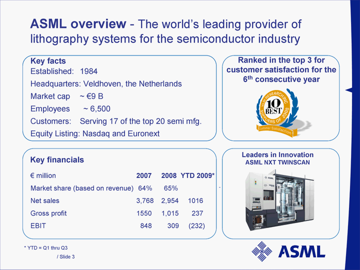
| ASML overview - The world's leading provider of lithography systems for the semiconductor industry Established: 1984 Headquarters: Veldhoven, the Netherlands Market cap ~ €9 B Employees ~ 6,500 Customers: Serving 17 of the top 20 semi mfg. Equity Listing: Nasdaq and Euronext Key facts Key financials € million 2007 2008 YTD 2009* Market share (based on revenue) 64% 65% - Net sales 3,768 2,954 1016 Gross profit 1550 1,015 237 EBIT 848 309 (232) Leaders in Innovation ASML NXT TWINSCAN Ranked in the top 3 for customer satisfaction for the 6th consecutive year * YTD = Q1 thru Q3 |
| Market Update |
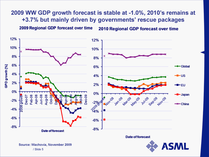
| 2009 WW GDP growth forecast is stable at -1.0%, 2010's remains at +3.7% but mainly driven by governments' rescue packages Source: Wachovia, November 2009 |
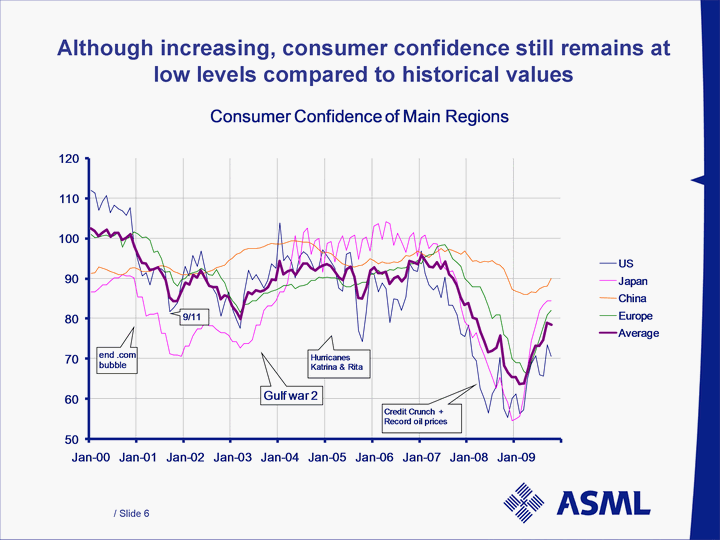
| Although increasing, consumer confidence still remains at low levels compared to historical values |
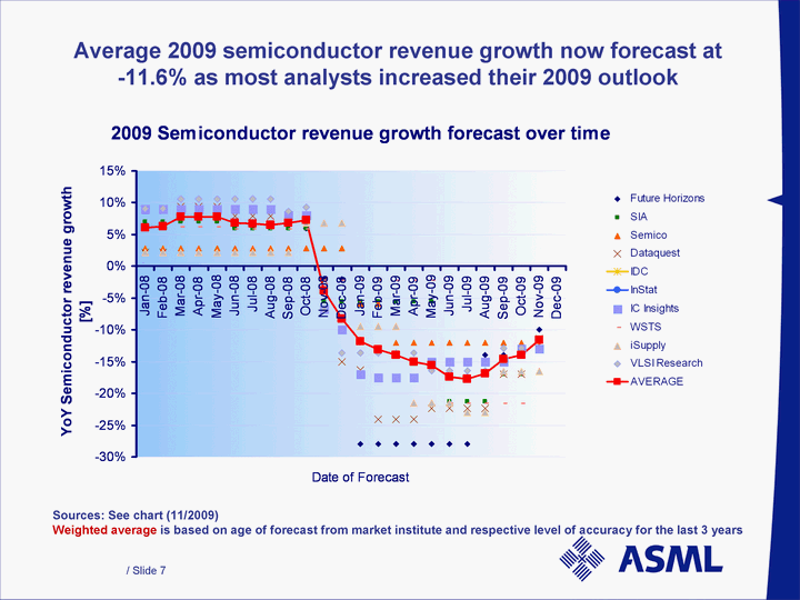
| Average 2009 semiconductor revenue growth now forecast at - -11.6% as most analysts increased their 2009 outlook Sources: See chart (11/2009) Weighted average is based on age of forecast from market institute and respective level of accuracy for the last 3 years |
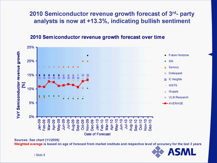
| 2010 Semiconductor revenue growth forecast of 3rd- party analysts is now at +13.3%, indicating bullish sentiment Sources: See chart (11/2009) Weighted average is based on age of forecast from market institute and respective level of accuracy for the last 3 years |
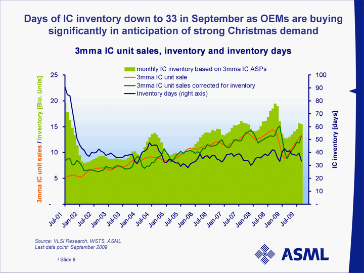
| Days of IC inventory down to 33 in September as OEMs are buying significantly in anticipation of strong Christmas demand Source: VLSI Research, WSTS, ASML Last data point: September 2009 |
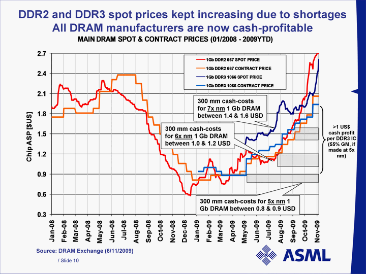
| Source: DRAM Exchange (6/11/2009) DDR2 and DDR3 spot prices kept increasing due to shortages All DRAM manufacturers are now cash-profitable 300 mm cash-costs for 5x nm 1 Gb DRAM between 0.8 & 0.9 USD 300 mm cash-costs for 7x nm 1 Gb DRAM between 1.4 & 1.6 USD 300 mm cash-costs for 6x nm 1 Gb DRAM between 1.0 & 1.2 USD >1 US$ cash profit per DDR3 IC (55% GM, if made at 5x nm) |
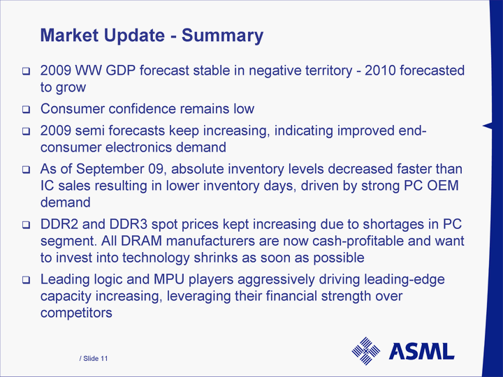
| Market Update - Summary 2009 WW GDP forecast stable in negative territory - 2010 forecasted to grow Consumer confidence remains low 2009 semi forecasts keep increasing, indicating improved end- consumer electronics demand As of September 09, absolute inventory levels decreased faster than IC sales resulting in lower inventory days, driven by strong PC OEM demand DDR2 and DDR3 spot prices kept increasing due to shortages in PC segment. All DRAM manufacturers are now cash-profitable and want to invest into technology shrinks as soon as possible Leading logic and MPU players aggressively driving leading-edge capacity increasing, leveraging their financial strength over competitors |
| Litho Technology |
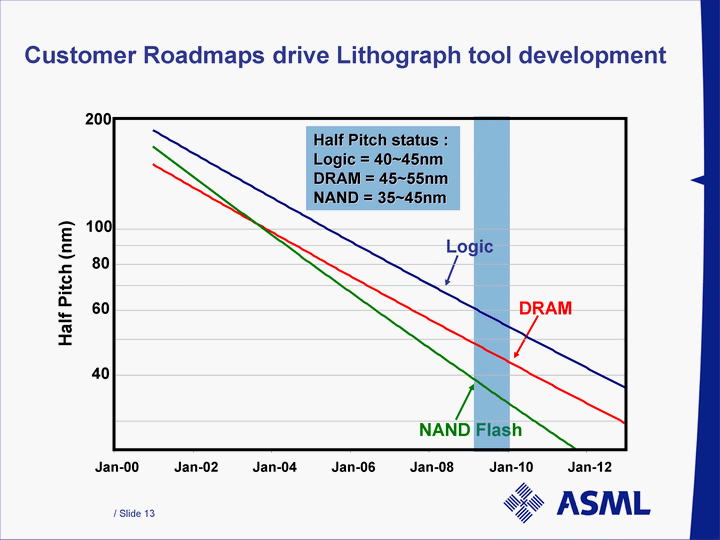
| NAND Flash Customer Roadmaps drive Lithograph tool development Jan-00 Jan-02 Jan-04 Jan-06 Jan-08 Jan-10 Jan-12 Half Pitch (nm) 200 100 80 60 40 Logic DRAM Half Pitch status : Logic = 40~45nm DRAM = 45~55nm NAND = 35~45nm |
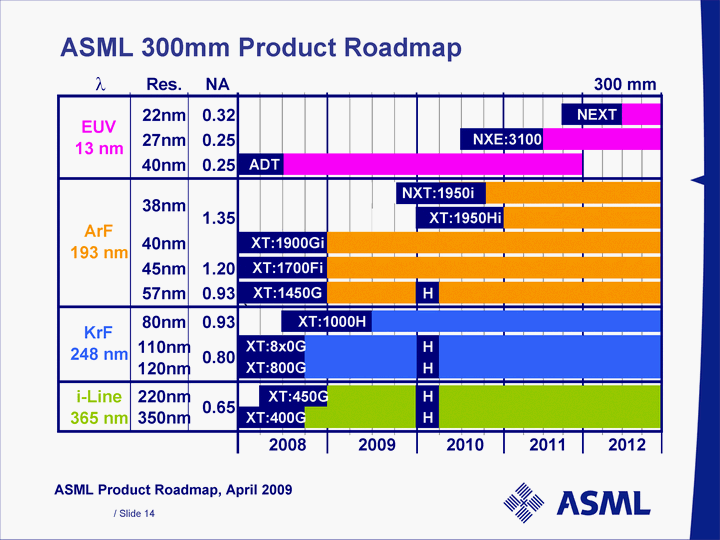
| ASML 300mm Product Roadmap l Res. NA 300 mm 22nm 0.32 27nm 0.25 40nm 0.25 40nm 45nm 1.20 57nm 0.93 H ' 80nm 0.93 110nm H 120nm H ASML Product Roadmap, April 2009 XT:1950Hi NXE:3100 NEXT XT:1450G 38nm EUV 13 nm ADT H ArF 193 nm 1.35 XT:1900Gi XT:1700Fi H KrF 248 nm XT:1000H 0.80 XT:8x0G XT:800G i-Line 365 nm 220nm 0.65 350nm XT:450G XT:400G 2012 2008 2009 2010 2011 NXT:1950i |
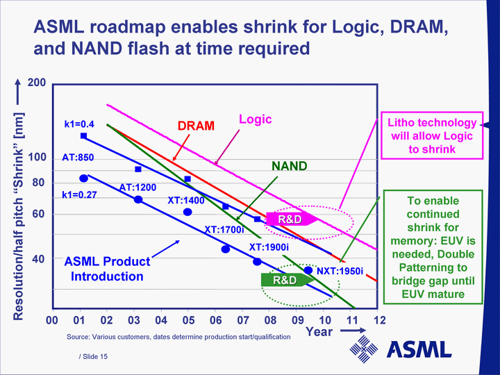
| ASML roadmap enables shrink for Logic, DRAM, and NAND flash at time required Source: Various customers, dates determine production start/qualification 10 12 200 100 80 60 40 11 07 09 08 04 06 05 01 03 02 00 Resolution/half pitch "Shrink" [nm] Year ASML Product Introduction XT:1400 XT:1700i AT:1200 AT:850 XT:1900i k1=0.4 k1=0.27 Logic DRAM R&D R&D NAND NXT:1950i |
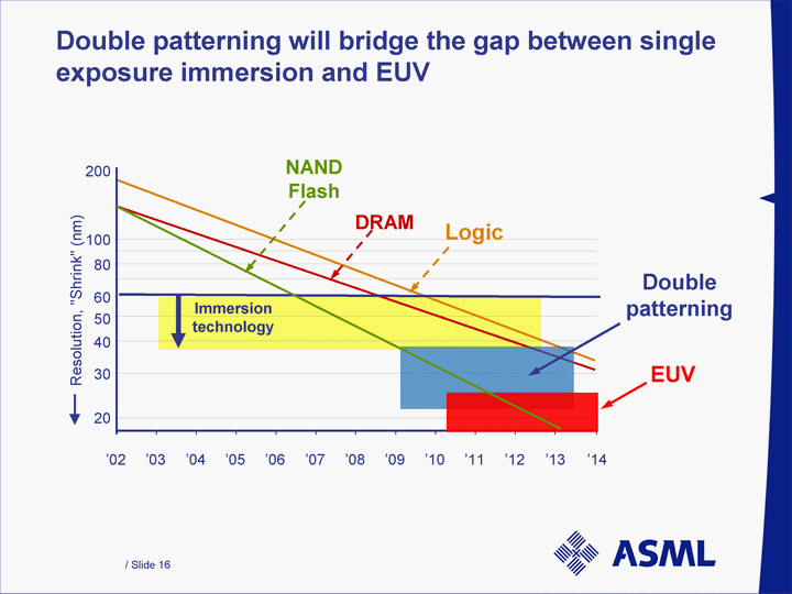
| Double patterning will bridge the gap between single exposure immersion and EUV '02 '03 '04 '05 '06 '07 '08 '09 '10 '11 '12 '13 '14 Resolution, "Shrink" (nm) 100 80 60 40 Logic NAND Flash DRAM 30 20 50 200 Immersion technology Double patterning EUV |
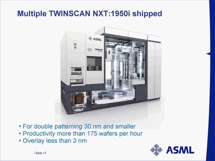
| For double patterning 30 nm and smaller Productivity more than 175 wafers per hour Overlay less than 3 nm Multiple TWINSCAN NXT:1950i shipped |
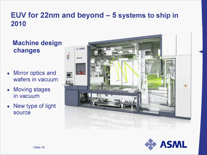
| EUV for 22nm and beyond - 5 systems to ship in 2010 Machine design changes Mirror optics and wafers in vacuum Moving stages in vacuum New type of light source |
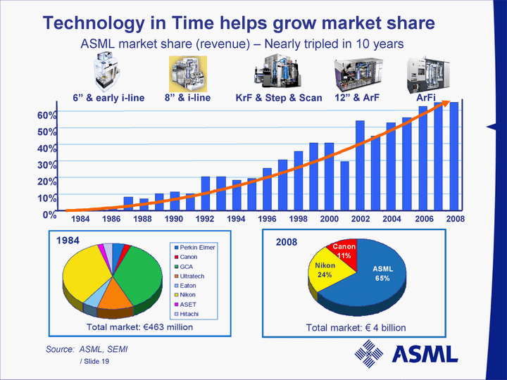
| Source: ASML, SEMI Source: ASML, SEMI 0% 10% 20% 30% 40% 50% 60% 1984 1986 1988 1990 1992 1994 1996 1998 2000 2002 2004 2006 2008 2008 8" & i-line 6" & early i-line KrF & Step & Scan 12" & ArF ArFi Technology in Time helps grow market share ASML market share (revenue) - Nearly tripled in 10 years |
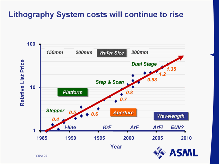
| 1 10 100 1985 1990 1995 2000 2005 2010 Year Lithography System costs will continue to rise Relative List Price i-line 300mm 200mm 150mm KrF ArF ArFi EUV? Wafer Size Wavelength Stepper Platform Step & Scan Dual Stage 0.4 0.5 0.6 0.7 0.8 0.93 1.2 1.35 Aperture |
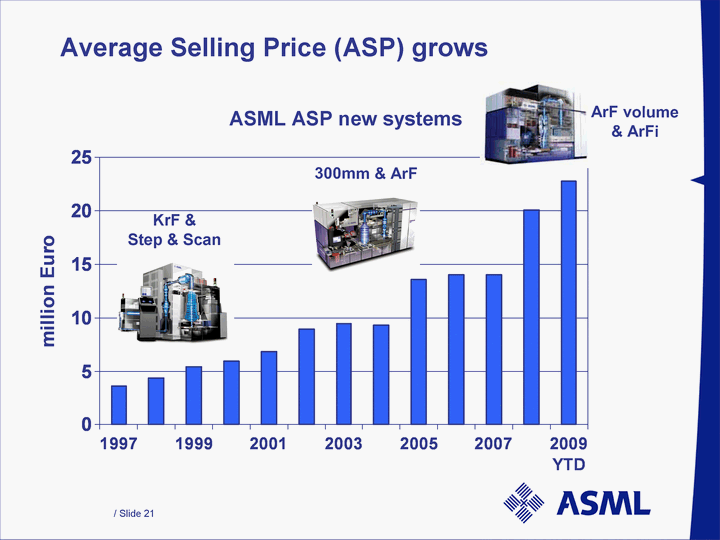
| Average Selling Price (ASP) grows 1997 1998 1999 2000 2001 2002 2003 2004 2005 2006 2007 2008 2009 YTD 3.59 4.38 5.4 5.9 6.8 8.92 9.46 9.28 13.54 14.01 14 20.03 22.75 MSGraph.Chart.8 MSGraph.Chart.8 ASML ASP new systems KrF & Step & Scan 300mm & ArF 300mm & ArF ArF volume & ArFi |
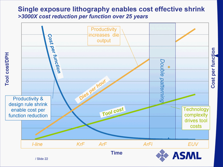
| Single exposure lithography enables cost effective shrink >3000X cost reduction per function over 25 years Time Tool cost/DPH Double patterning I-line KrF ArF ArFi EUV Tool cost Dies per hour Cost per function Cost per function |
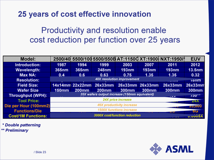
| Model: 2500/40 5500/100 5500/550B AT:1150C XT:1900i NXT:1950i* EUV Introduction: 1987 1994 1999 2003 2007 2011 2012 Wavelength: 365nm 365nm 248nm 193nm 193nm 193nm 13.5nm Max NA: 0.4 0.6 0.63 0.75 1.35 1.35 0.32 Resolution: 0.7µm 0.35µm 0.18µm 90nm 40nm 32nm 18nm Field Size: 14x14mm 22x22mm 26x33mm 26x33mm 26x33mm 26x33mm 26x33mm Wafer Size 150mm 200mm 200mm 300mm 300mm 300mm 300mm Throughput (WPH): 17 55 94 103 131 100 150** Tool Price: 1.0X 1.25X 3.1X 6.25X 12.5X 16.5X 24X Die per Hour (100mm2): 2,000 14,000 25,000 64,000 81,000 62,000 93,000 Functions/Die 4M 16M 64M 256M 1.2G 2G 6G Cost/1M Functions: 1.0X 0.042X 0.015X 0.003X 0.001X 0.001X 0.0005X * Double patterning ** Preliminary 25 years of cost effective innovation Productivity and resolution enable cost reduction per function over 25 years 24X price increase 46X productivity increase 1500X functions increase 3000X cost/function reduction 35X wafers output increase (150mm equivalent) 40X resolution improvement |
| Summary The Semiconductor industry is in a transition phase due to the current severe worldwide financial crisis Shrinking design rules have been the economical driver of the IC industry. Lithography remains the key enabler Shrinking design rules require increasingly more sophisticated litho systems resulting in a steady growth in their cost and resulting ASP's ASML insures that the increasing cost of litho systems remain acceptable by developing solutions that result in maximum usable shrink while driving increased productivity to ensure steady improvement in cost per function Future lithography technologies will likely ensure that the economics of shrink remain attractive for several more generations |
