- ASML Dashboard
- Financials
- Filings
-
Holdings
- Transcripts
- ETFs
-
Insider
- Institutional
- Shorts
-
6-K Filing
ASML Holding (ASML) 6-KCurrent report (foreign)
Filed: 14 Jun 10, 12:00am
| 2010 UBS Global Technology and Services Conference Eric Meurice CEO New York, New York June 8, 2010 |
| Safe Harbor "Safe Harbor" Statement under the US Private Securities Litigation Reform Act of 1995: the matters discussed in this document may include forward-looking statements, including statements made about our outlook, realization of backlog, IC unit demand, financial results, average selling price, gross margin and expenses. These forward looking statements are subject to risks and uncertainties including, but not limited to: economic conditions, product demand and semiconductor equipment industry capacity, worldwide demand and manufacturing capacity utilization for semiconductors (the principal product of our customer base), including the impact of general economic conditions on consumer confidence and demand for our customers' products, competitive products and pricing, manufacturing efficiencies, new product development and customer acceptance of new products, ability to enforce patents and protect intellectual property rights, the risk of intellectual property litigation, availability of raw materials and critical manufacturing equipment, trade environment, changes in exchange rates and other risks indicated in the risk factors included in ASML's Annual Report on Form 20-F and other filings with the US Securities and Exchange Commission. |
| Agenda ASML Overview Short Term Business overview Future trends ASML Trajectory |
| ASML Overview |
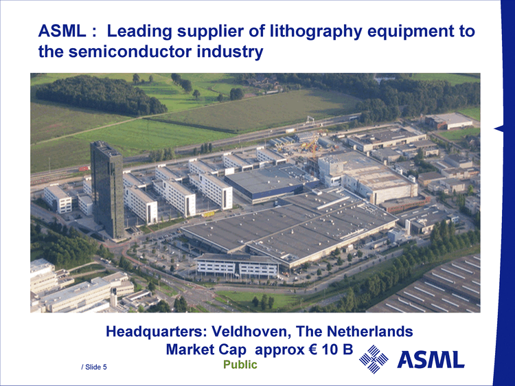
| ASML : Leading supplier of lithography equipment to the semiconductor industry Headquarters: Veldhoven, The Netherlands Market Cap approx € 10 B |
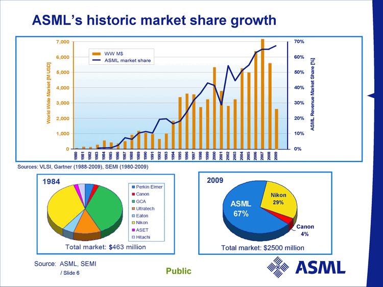
| Source: ASML, SEMI ASML's historic market share growth 0% 10% 20% 30% 40% 50% 60% 1984 1986 1988 1990 1992 1994 1996 1998 2000 2002 2004 2006 2008 Total market: $2500 million 2009 70% Sources: VLSI, Gartner (1988-2009), SEMI (1980-2009) $ 1,000 2,000 3,000 4,000 5,000 6,000 7,000 1980 2005 2007 World Wide Market [M USD] 2009 1982 1990 1997 1986 1993 1995 1999 2001 2003 2006 2008 1984 1992 1998 1988 1994 1996 2000 2002 2004 1981 1983 1991 1987 1985 1989 WW M$ ASML market share WW M$ ASML market share 0 0% 10% 20% 30% 40% 50% 60% 70% ASML Revenue Market Share [%] 0% 10% 20% 30% 40% 50% 60% 70% ASML Revenue Market Share [%] 0% 10% 20% 30% 40% 50% 60% 70% ASML Revenue Market Share [%] 0% 10% 20% 30% 40% 50% 60% 70% ASML Revenue Market Share [%] 0% 10% 20% 30% 40% 50% 60% 70% ASML Revenue Market Share [%] 0% 10% 20% 30% 40% 50% 60% 70% ASML Revenue Market Share [%] Nikon 29% Canon 4% ASML 67% |
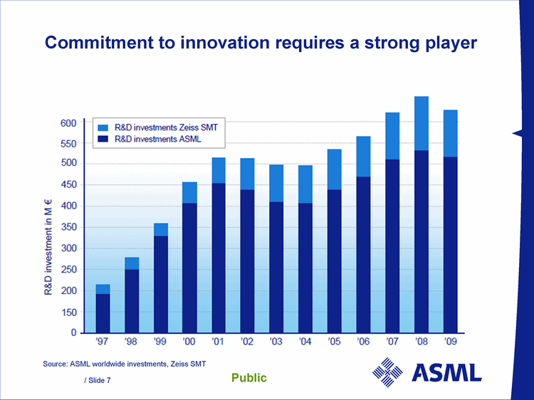
| Commitment to innovation requires a strong player Source: ASML worldwide investments, Zeiss SMT |
| Short Term Business overview |
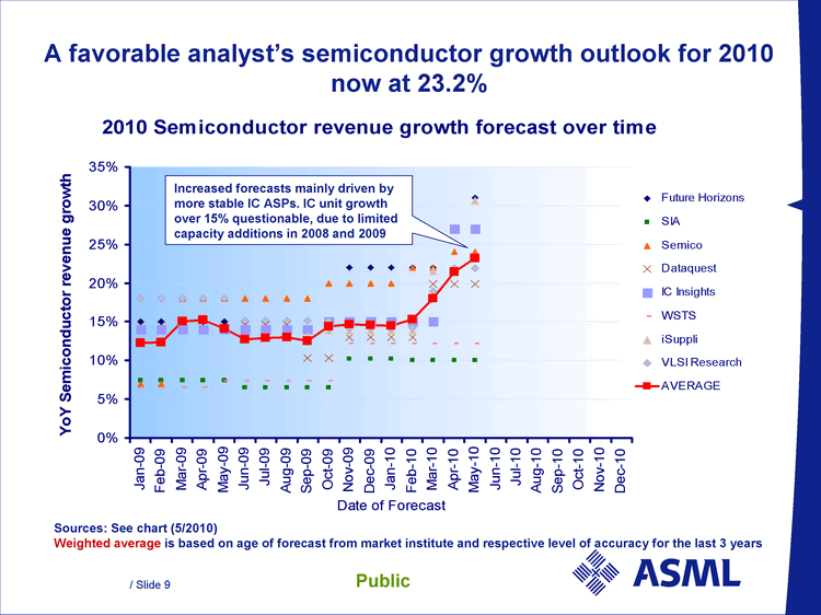
| A favorable analyst's semiconductor growth outlook for 2010 now at 23.2% Sources: See chart (5/2010) Weighted average is based on age of forecast from market institute and respective level of accuracy for the last 3 years Increased forecasts mainly driven by more stable IC ASPs. IC unit growth over 15% questionable, due to limited capacity additions in 2008 and 2009 2010 Semiconductor revenue growth forecast over time 0% 5% 10% 15% 20% 25% 30% 35% Jan-09 Feb-09 Mar-09 Apr-09 May-09 Jun-09 Jul-09 Aug-09 Sep-09 Oct-09 Nov-09 Dec-09 Jan-10 Feb-10 Mar-10 Apr-10 May-10 Jun-10 Jul-10 Aug-10 Sep-10 Oct-10 Nov-10 Dec-10 Date of Forecast YoY Semiconductor revenue growth Future Horizons SIA Semico Dataquest IC Insights WSTS iSuppli VLSI Research AVERAGE |
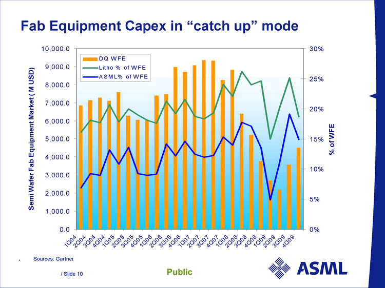
| Fab Equipment Capex in "catch up" mode Sources: Gartner 0.0 1,000.0 2,000.0 3,000.0 4,000.0 5,000.0 6,000.0 7,000.0 8,000.0 9,000.0 10,000.0 1Q04 2Q04 3Q04 4Q04 1Q05 2Q05 3Q05 4Q05 1Q06 2Q06 3Q06 4Q06 1Q07 2Q07 3Q07 4Q07 1Q08 2Q08 3Q08 4Q08 1Q09 2Q09 3Q09 4Q09 Semi Wafer Fab Equipment Market ( M USD) 0% 5% 10% 15% 20% 25% 30% % of WFE DQ WFE Litho % of WFE ASML% of WFE |
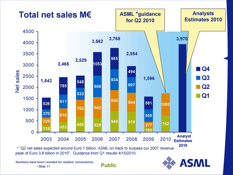
| Total net sales M€ 1,543 2,465 2,529 3,582 3,768 Numbers have been rounded for readers' convenience. 2,954 1,596 ASML *guidance for Q2 2010 * "Q2 net sales expected around Euro 1 billion. ASML on track to surpass our 2007 revenue peak of Euro 3.8 billion in 2010". Guidance from Q1 results 4/15/2010 Analyst Estimates 2010 Analysts Estimates 2010 3,970 318 453 685 629 949 919 183 742 329 616 763 942 930 844 277 1000 370 611 533 958 934 697 555 526 785 548 1053 955 494 581 0 500 1000 1500 2000 2500 3000 3500 4000 4500 2003 2004 2005 2006 2007 2008 2009 2010 Net sales Q4 Q3 Q2 Q1 |
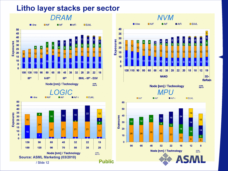
| NVM MPU DRAM LOGIC Litho layer stacks per sector Source: ASML Marketing (03/2010) 14 14 13 13 18 17 15 13 13 16 16 15 15 15 9 11 12 12 9 8 10 11 11 11 11 12 12 12 4 4 7 9 4 5 5 5 5 5 5 5 7 7 9 9 11 9 9 5 1 1 4 0 5 10 15 20 25 30 35 40 45 50 150 130 110 90 80 65 55 45 38 32 28 25 22 18 8F2 6-8F2 6F2 BWL - 6F2 - EUV Node [nm] / Technology Exposures I-line KrF ArF ArFi EUVL ASML Mar-10 17 16 15 11 11 10 10 9 9 9 9 9 9 9 10 11 12 10 13 13 12 13 13 13 13 13 13 13 13 12 3 4 4 2 2 3 3 3 3 3 3 3 6 3 4 4 6 7 7 6 6 6 5 1 1 1 5 0 5 10 15 20 25 30 35 40 130 110 90 80 65 55 42 35 28 22 20 18 15 12 19 NAND 3D- ReRam Node [nm] / Technology Exposures I-line KrF ArF ArFi EUVL ASML Mar-10 18 7 2 2 2 2 2 15 24 20 21 21 21 17 4 16 1 4 16 16 22 5 12 0 5 10 15 20 25 30 35 40 45 50 130 90 65 45 32 22 15 150 120 90 70 50 35 25 Node [nm] / Technology Exposures I-line KrF ArF ArF-i EUVL ASML Mar-10 26 26 30 26 23 13 9 6 10 12 11 4 5 14 14 5 12 18 24 14 14 14 18 0 10 20 30 40 50 60 90 65 45 32 22 16 12 8 Node [nm] / Technology Exposures KrF ArF ArF-i EUVL ASML Mar-10 |
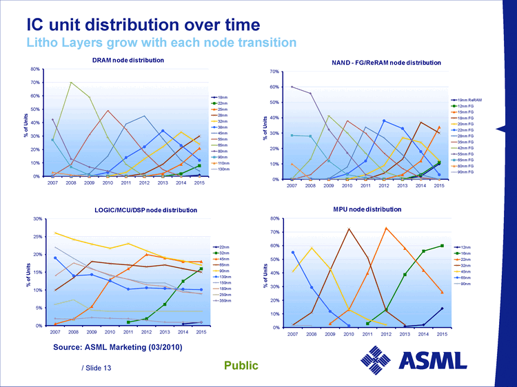
| IC unit distribution over time Litho Layers grow with each node transition Source: ASML Marketing (03/2010) 0% 10% 20% 30% 40% 50% 60% 70% 80% 2007 2008 2009 2010 2011 2012 2013 2014 2015 % of Units DRAM node distribution 18nm 22nm 25nm 28nm 32nm 38nm 45nm 55nm 65nm 80nm 90nm 110nm 130nm 0% 10% 20% 30% 40% 50% 60% 70% 2007 2008 2009 2010 2011 2012 2013 2014 2015 % of Units NAND - - FG/ReRAM node distribution 19nm ReRAM 12nm FG 15nm FG 18nm FG 20nm FG 22nm FG 28nm FG 35nm FG 42nm FG 55nm FG 65nm FG 80nm FG 90nm FG 0% 5% 10% 15% 20% 25% 30% 2007 2008 2009 2010 2011 2012 2013 2014 2015 % of Units LOGIC/MCU/DSP node distribution 22nm 32nm 45nm 65nm 90nm 130nm 150nm 180nm 250nm 350nm 0% 10% 20% 30% 40% 50% 60% 70% 80% 2007 2008 2009 2010 2011 2012 2013 2014 2015 % of Units MPU node distribution 12nm 16nm 22nm 32nm 45nm 65nm 90nm |
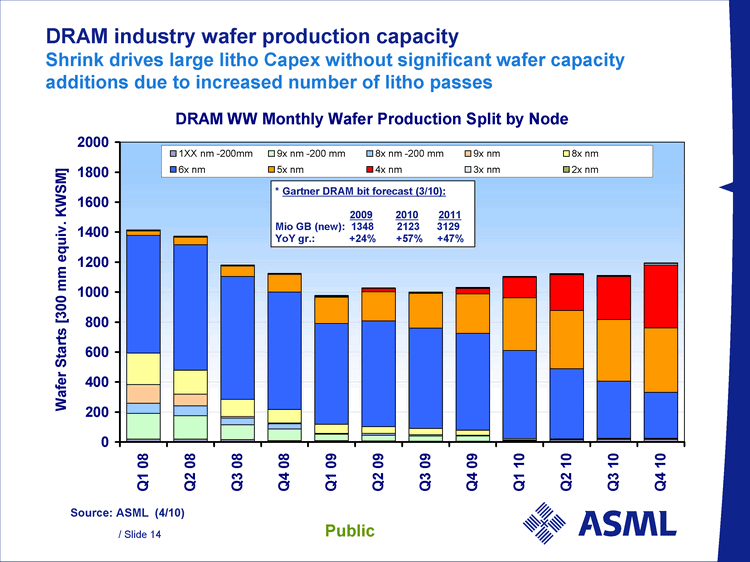
| Source: ASML (4/10) * Gartner DRAM bit forecast (3/10): 2009 2010 2011 Mio GB (new): 1348 2123 3129 YoY gr.: +24% +57% +47% DRAM industry wafer production capacity Shrink drives large litho Capex without significant wafer capacity additions due to increased number of litho passes DRAM WW Monthly Wafer Production Split by Node 0 200 400 600 800 1000 1200 1400 1600 1800 2000 Q1 08 Q2 08 Q3 08 Q4 08 Q1 09 Q2 09 Q3 09 Q4 09 Q1 10 Q2 10 Q3 10 Q4 10 Wafer Starts [300 mm equiv. KWSM] 1XX nm -200mm 9x nm -200 mm 8x nm -200 mm 9x nm 8x nm 6x nm 5x nm 4x nm 3x nm 2x nm |
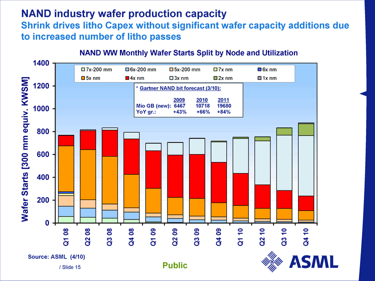
| Source: ASML (4/10) * Gartner NAND bit forecast (3/10): 2009 2010 2011 Mio GB (new): 6467 10718 19680 YoY gr.: +43% +66% +84% NAND industry wafer production capacity Shrink drives litho Capex without significant wafer capacity additions due to increased number of litho passes NAND WW Monthly Wafer Starts Split by Node and Utilization 0 200 400 600 800 1000 1200 1400 Q1 08 Q2 08 Q3 08 Q4 08 Q1 09 Q2 09 Q3 09 Q4 09 Q1 10 Q2 10 Q3 10 Q4 10 Wafer Starts [300 mm equiv. KWSM] 7x-200 mm 6x-200 mm 5x-200 mm 7x nm 6x nm 5x nm 4x nm 3x nm 2x nm 1x nm |
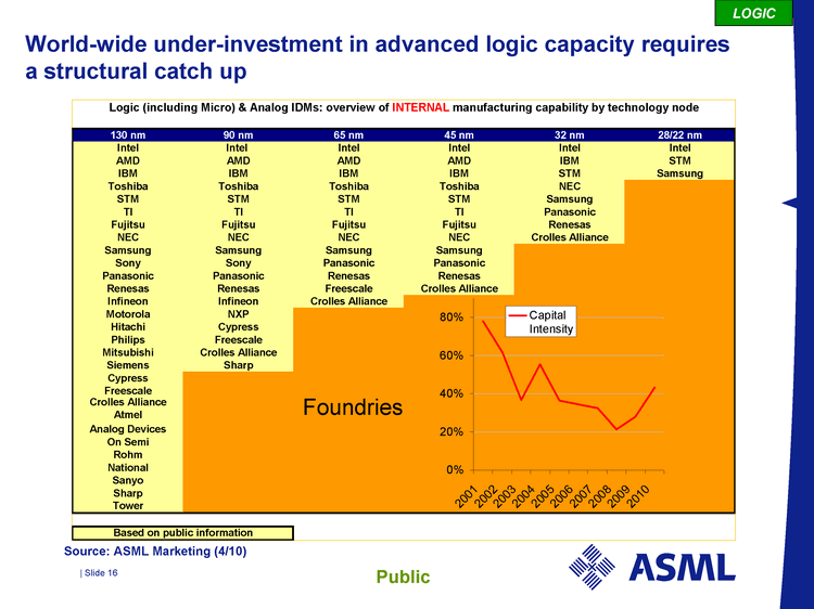
| World-wide under-investment in advanced logic capacity requires a structural catch up Source: ASML Marketing (4/10) LOGIC Foundries 130 nm 90 nm 65 nm 45 nm 32 nm 28/22 nm Intel Intel Intel Intel Intel Intel AMD AMD AMD AMD IBM STM IBM IBM IBM IBM STM Samsung Toshiba Toshiba Toshiba Toshiba NEC STM STM STM STM Samsung TI TI TI TI Panasonic Fujitsu Fujitsu Fujitsu Fujitsu Renesas NEC NEC NEC NEC Crolles Alliance Samsung Samsung Samsung Samsung Sony Sony Panasonic Panasonic Panasonic Panasonic Renesas Renesas Renesas Renesas Freescale Crolles Alliance Infineon Infineon Crolles Alliance Motorola NXP Hitachi Cypress Philips Freescale Mitsubishi Crolles Alliance Siemens Sharp Cypress Freescale Crolles Alliance Atmel Analog Devices On Semi Rohm National Sanyo Sharp Tower Based on public information FOUNDRIES Logic (including Micro) & Analog IDMs: overview of INTERNAL manufacturing capability by technology node |
| Future trends |
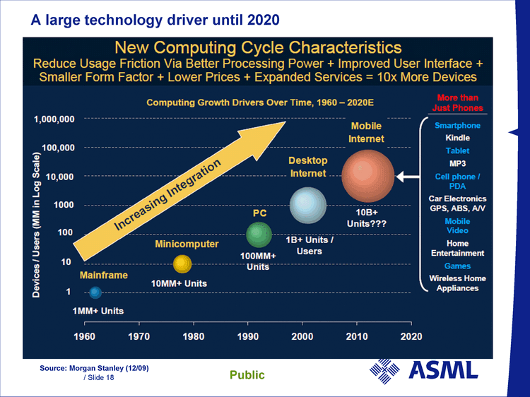
| A large technology driver until 2020 Source: Morgan Stanley (12/09) |
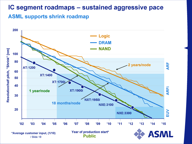
| IC segment roadmaps - sustained aggressive pace ASML supports shrink roadmap Year of production start* Resolution/half pitch, "Shrink" [nm] 20 30 40 50 60 80 200 100 '02 '03 '04 '05 '06 '07 '08 '09 '10 '11 '12 '13 '14 '15 ARF ARFi EUV Logic *Average customer input, (1/10) NAND DRAM XT:1400 XT:1700i AT:1200 XT:1900i NXT:1950i NXE:3100 NXE:3300 2 years/node 18 months/node 1 year/node |
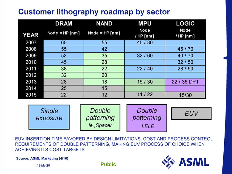
| Customer lithography roadmap by sector EUV Single exposure Double patterning ie.,Spacer Double patterning LELE Source: ASML Marketing (4/10) EUV INSERTION TIME FAVORED BY DESIGN LIMITATIONS, COST AND PROCESS CONTROL REQUIREMENTS OF DOUBLE PATTERNING, MAKING EUV PROCESS OF CHOICE WHEN ACHIEVING ITS COST TARGETS 15/30 YEAR 2007 2008 2009 2010 2011 2012 2013 2014 2015 11 / 22 LOGIC Node / HP [nm] 45 / 70 40 / 70 22 / 40 32 / 50 22 / 35 DPT 15 / 30 28 / 50 MPU Node / HP [nm] 45 / 80 32 / 60 DRAM 65 NAND 55 Node = HP [nm] Node = HP [nm] 22 28 42 35 55 52 22 18 12 28 38 25 20 15 32 45 |
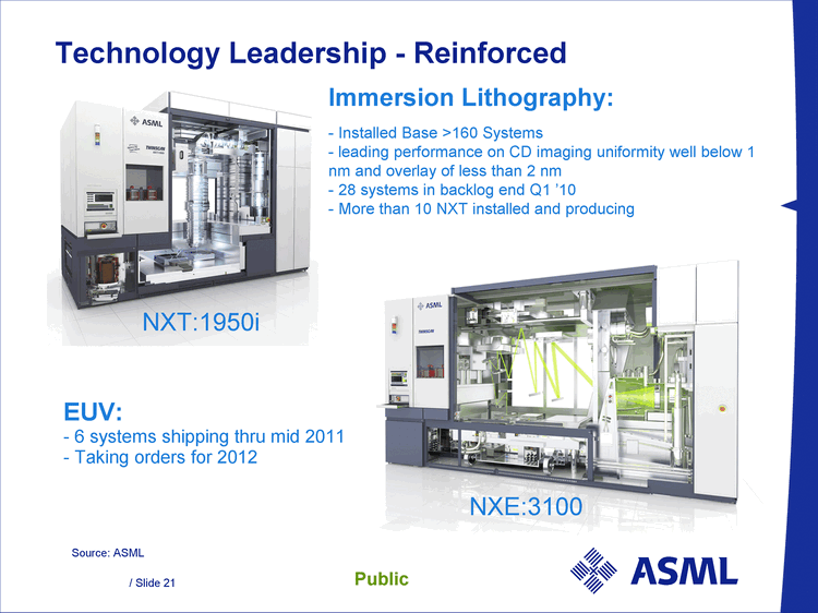
| Technology Leadership - Reinforced Source: ASML Immersion Lithography: Installed Base >160 Systems leading performance on CD imaging uniformity well below 1 nm and overlay of less than 2 nm 28 systems in backlog end Q1 '10 More than 10 NXT installed and producing EUV: - - 6 systems shipping thru mid 2011 - - Taking orders for 2012 NXT:1950i NXE:3100 |
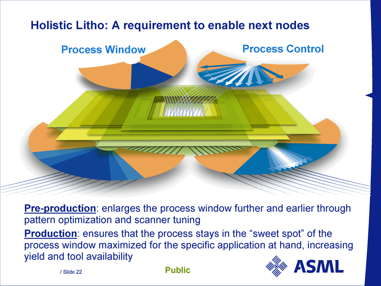
| Holistic Litho: A requirement to enable next nodes Pre-production: enlarges the process window further and earlier through pattern optimization and scanner tuning Production: ensures that the process stays in the "sweet spot" of the process window maximized for the specific application at hand, increasing yield and tool availability Process Window Process Control |
| Summary |
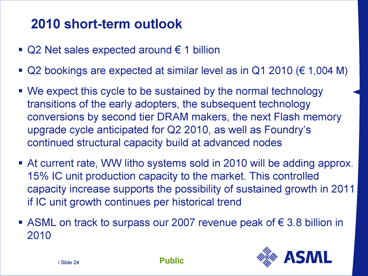
| 2010 short-term outlook Q2 Net sales expected around € 1 billion Q2 bookings are expected at similar level as in Q1 2010 (€ 1,004 M) We expect this cycle to be sustained by the normal technology transitions of the early adopters, the subsequent technology conversions by second tier DRAM makers, the next Flash memory upgrade cycle anticipated for Q2 2010, as well as Foundry's continued structural capacity build at advanced nodes At current rate, WW litho systems sold in 2010 will be adding approx. 15% IC unit production capacity to the market. This controlled capacity increase supports the possibility of sustained growth in 2011 if IC unit growth continues per historical trend ASML on track to surpass our 2007 revenue peak of € 3.8 billion in 2010 |
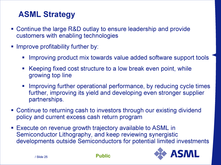
| ASML Strategy Continue the large R&D outlay to ensure leadership and provide customers with enabling technologies Improve profitability further by: Improving product mix towards value added software support tools Keeping fixed cost structure to a low break even point, while growing top line Improving further operational performance, by reducing cycle times further, improving its yield and developing even stronger supplier partnerships. Continue to returning cash to investors through our existing dividend policy and current excess cash return program Execute on revenue growth trajectory available to ASML in Semiconductor Lithography, and keep reviewing synergistic developments outside Semiconductors for potential limited investments |
| ASML Trajectory ASML confirms its leadership in offering lithography technology that enables the industry's shrink roadmaps and therefore makes ASML the partner of choice for all leading Semiconductor manufacturers ASML confirms that it has the appropriate size and know how to continue leading the industry through 2015 and beyond in a Lithography market which supports ASML's target for 5B Euro revenues at current cycle peak. |
