- ASML Dashboard
- Financials
- Filings
-
Holdings
- Transcripts
- ETFs
-
Insider
- Institutional
- Shorts
-
6-K Filing
ASML Holding (ASML) 6-KCurrent report (foreign)
Filed: 28 Mar 11, 12:00am
| Taiwan, Technology and Beyond Conference Bank of America Merrill Lynch Craig DeYoung - VP Investor Relations Taipei, Taiwan March 15, 2011 |
| Safe Harbor "Safe Harbor" Statement under the US Private Securities Litigation Reform Act of 1995: the matters discussed in this document may include forward-looking statements, including statements made about our outlook, realization of backlog, IC unit demand, financial results, average selling price, gross margin and expenses, dividend policy and intention to repurchase shares. These forward looking statements are subject to risks and uncertainties including, but not limited to: economic conditions, product demand and semiconductor equipment industry capacity, worldwide demand and manufacturing capacity utilization for semiconductors (the principal product of our customer base), including the impact of general economic conditions on consumer confidence and demand for our customers' products, competitive products and pricing, the impact of manufacturing efficiencies and capacity constraints, the pace of new product development and customer acceptance of new products, our ability to enforce patents and protect intellectual property rights, the risk of intellectual property litigation, availability of raw materials and critical manufacturing equipment, trade environment, changes in exchange rates, available cash, distributable reserves for dividend payments and share repurchases and other risks indicated in the risk factors included in ASML's Annual Report on Form 20-F and other filings with the US Securities and Exchange Commission. |

| Agenda ASML overview Market update ASML business update Outlook and summary |
| ASML Overview |
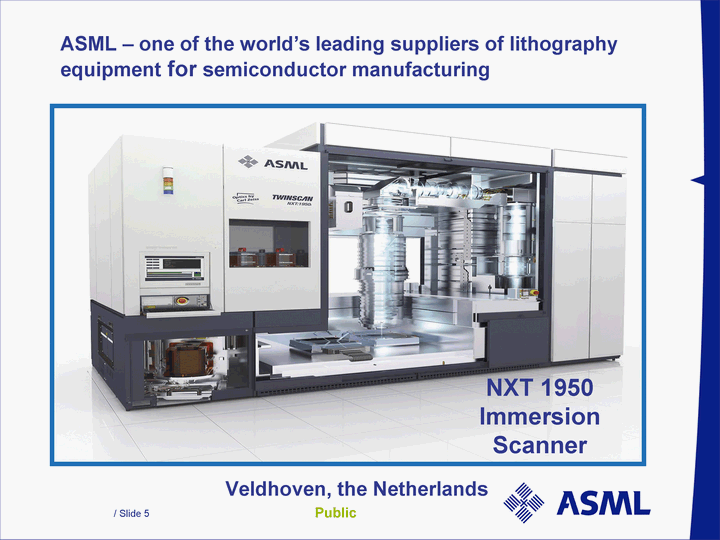
| ASML - one of the world's leading suppliers of lithography equipment for semiconductor manufacturing equipment for semiconductor manufacturing equipment for semiconductor manufacturing Veldhoven, the Netherlands Veldhoven, the Netherlands NXT 1950 Immersion Scanner |
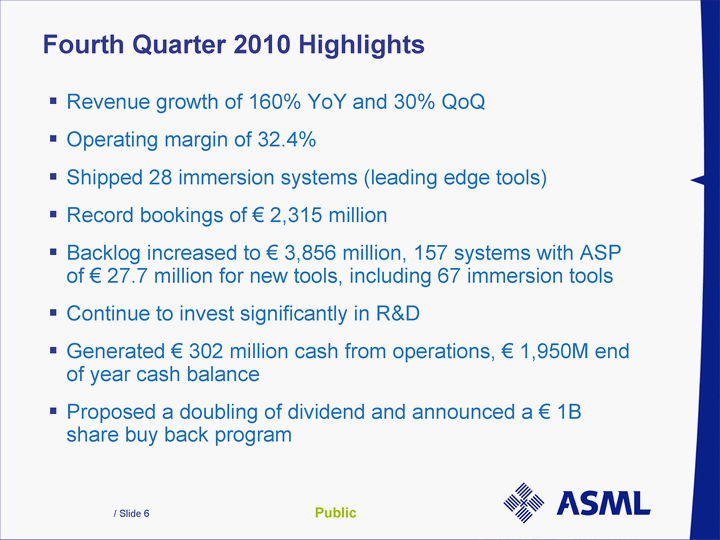
| Fourth Quarter 2010 Highlights Revenue growth of 160% YoY and 30% QoQ Operating margin of 32.4% Shipped 28 immersion systems (leading edge tools) Record bookings of € 2,315 million Backlog increased to € 3,856 million, 157 systems with ASP of € 27.7 million for new tools, including 67 immersion tools Continue to invest significantly in R&D Generated € 302 million cash from operations, € 1,950M end of year cash balance Proposed a doubling of dividend and announced a € 1B share buy back program |
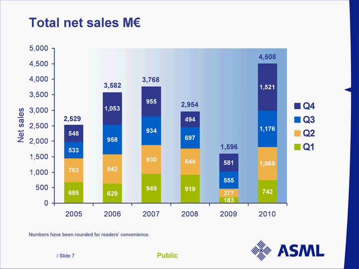
| 2005 2006 2007 2008 2009 2010 Q1 685 629 949 919 183 742 Q2 763 942 930 844 277 1069 Q3 533 958 934 697 555 1176 Q4 548 1053 955 494 581 1521 Total net sales M€ 2,529 3,582 3,768 Numbers have been rounded for readers' convenience. 2,954 1,596 4,508 |
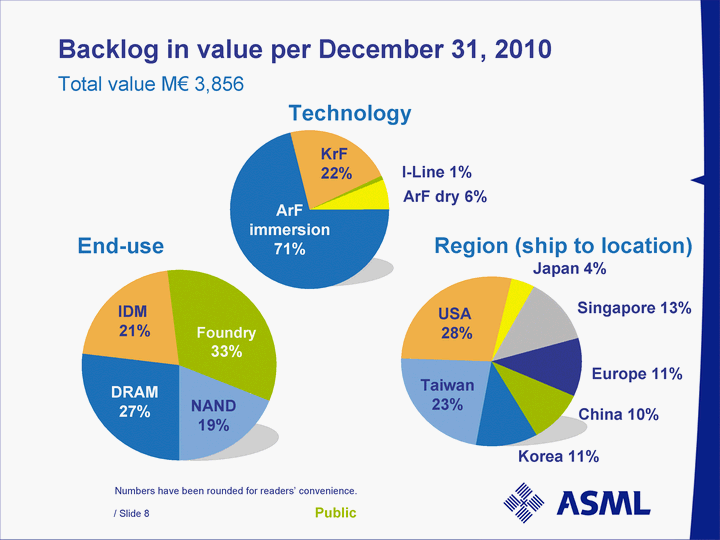
| Korea Taiwan USA Japan Singapore Europe China 11 23 28 4 13 11 10 DRAM IDM Foundry NAND 27 21 33 0 19 0 immersion KrF 1-line ArF dry 71 22 1 6 Backlog in value per December 31, 2010 Total value M€ 3,856 Technology ArF immersion 71% KrF 22% I-Line 1% Region (ship to location) USA 28% Taiwan 23% Korea 11% Europe 11% Japan 4% End-use DRAM 27% IDM 21% Foundry 33% Numbers have been rounded for readers' convenience. Singapore 13% China 10% ArF dry 6% NAND 19% |
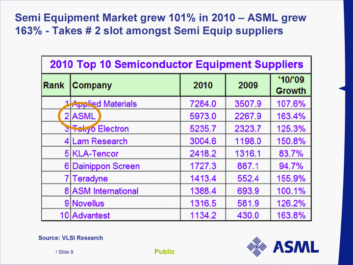
| Semi Equipment Market grew 101% in 2010 - ASML grew 163% - Takes # 2 slot amongst Semi Equip suppliers 163% - Takes # 2 slot amongst Semi Equip suppliers 163% - Takes # 2 slot amongst Semi Equip suppliers Source: VLSI Research |
| Market Update |
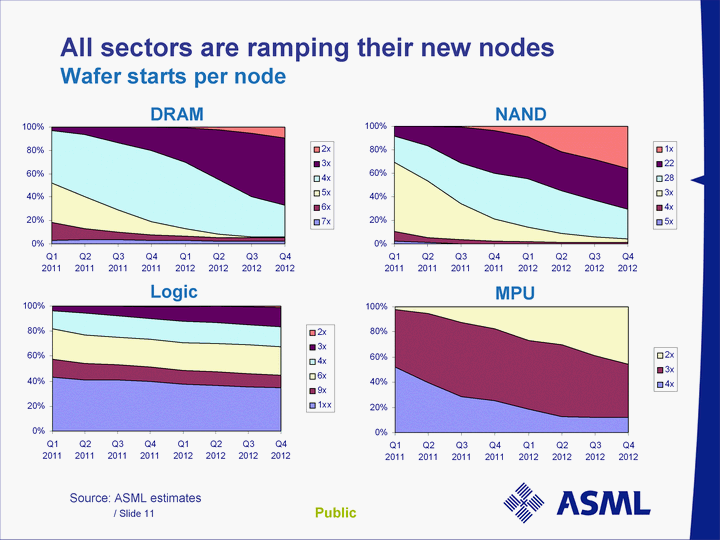
| All sectors are ramping their new nodes Wafer starts per node Wafer starts per node Wafer starts per node DRAM NAND Logic MPU Source: ASML estimates |
| Memory |
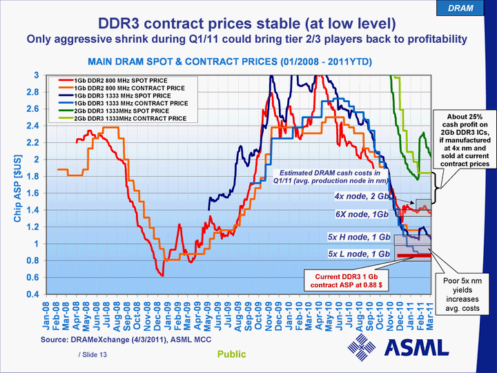
| Source: DRAMeXchange (4/3/2011), ASML MCC DDR3 contract prices stable (at low level) Only aggressive shrink during Q1/11 could bring tier 2/3 players back to profitability DRAM 6X node, 1Gb 5x H node, 1 Gb 5x L node, 1 Gb 4x node, 2 Gb Estimated DRAM cash costs in Q1/11 (avg. production node in nm) Current DDR3 1 Gb contract ASP at 0.88 $ Poor 5x nm yields increases avg. costs About 25% cash profit on 2Gb DDR3 ICs, if manufactured at 4x nm and sold at current contract prices |
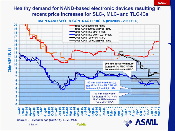
| NAND 300 mm cash-costs for 3x nm 32 Gb 2 b/c MLC NAND between 3,2 and 4,0 USD Healthy demand for NAND-based electronic devices resulting in recent price increases for SLC-, MLC- and TLC-ICs Source: DRAMeXchange (4/3/2011), ASML MCC 300 mm cash-costs for 3x nm 32 Gb 3 b/c MLC NAND between 2,6 and 3,2 USD 300 mm costs for mature 2x nm 64 Gb MLC NAND between 5.5 and 6,5 USD |
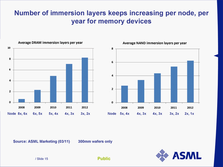
| Number of immersion layers keeps increasing per node, per year for memory devices Node 8x, 6x 6x, 5x 5x, 4x 4x, 3x 3x, 2x Node 5x, 4x 4x, 3x 4x, 3x 3x, 2x 2x, 1x 0 2 4 6 8 10 2008 2009 2010 2011 2012 Add. layers per year Immersion Exposures Average DRAM immersion layers per year 0 2 4 6 8 2008 2009 2010 2011 2012 Add. layers per year Immersion Exposures Average NAND immersion layers per year Source: ASML Marketing (03/11) 300mm wafers only |
| Logic |
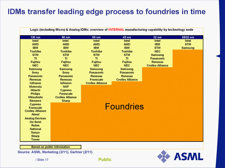
| IDMs transfer leading edge process to foundries in time Source: ASML Marketing (3/11), Gartner (2/11) Source: ASML Marketing (3/11), Gartner (2/11) Foundries |
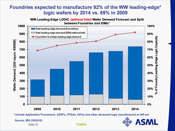
| Source: IBS (10/2010) Foundries expected to manufacture 92% of the WW leading-edge* logic wafers by 2014 vs. 69% in 2009 * Include Application Processors, ASSPs, FPGAs, GPUs and other advanced logic manufactured at ^90 nm done done |
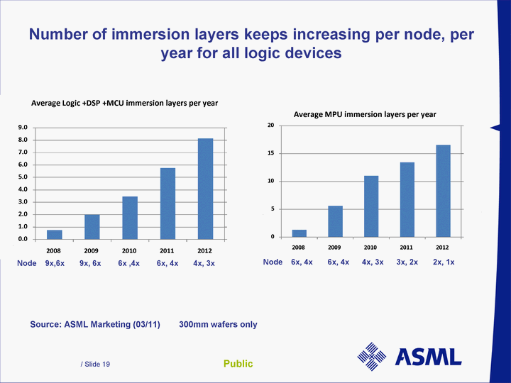
| Number of immersion layers keeps increasing per node, per year for all logic devices Source: ASML Marketing (03/11) 300mm wafers only Node 9x,6x 9x, 6x 6x ,4x 6x, 4x 4x, 3x Node 6x, 4x 6x, 4x 4x, 3x 3x, 2x 2x, 1x 0.0 1.0 2.0 3.0 4.0 5.0 6.0 7.0 8.0 9.0 2008 2009 2010 2011 2012 Add. layers per year [300mm only] Immersion Exposures [300mm only] Average Logic +DSP +MCU immersion layers per year 0 5 10 15 20 2008 2009 2010 2011 2012 Add. layers per year Immersion Exposures Average MPU immersion layers per year |
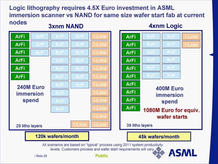
| Logic lithography requires 4.5X Euro investment in ASML immersion scanner vs NAND for same size wafer start fab at current nodes 45k wafers/month All scenarios are based on "typical" process using 2011 system productivity levels. Customers process and wafer start requirements will vary. 120k wafers/month 3xnm NAND 29 litho layers ArFi ArF KrF KrF ArF I-Line I-Line KrF KrF I-Line I-Line KrF I-Line I-Line I-Line ArFi ArFi ArFi ArFi I-Line I-Line I-Line KrF KrF ArFi KrF KrF KrF KrF KrF KrF KrF KrF KrF KrF I-Line I-Line I-Line ArF 240M Euro immersion spend 4xnm Logic ArFi 39 litho layers KrF KrF I-Line I-Line KrF KrF KrF KrF ArFi ArFi ArFi ArFi ArFi ArFi KrF KrF ArFi ArFi ArFi KrF KrF KrF KrF 400M Euro immersion spend 1080M Euro for equiv. wafer starts |
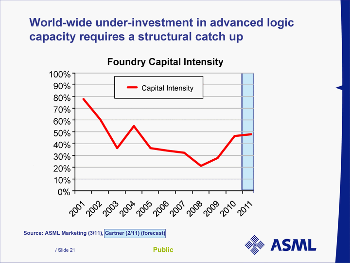
| World-wide under-investment in advanced logic capacity requires a structural catch up Source: ASML Marketing (3/11), Gartner (2/11) (forecast) 0% 10% 20% 30% 40% 50% 60% 70% 80% 90% 100% Capital Intensity Foundry Capital Intensity Capital Intensity |
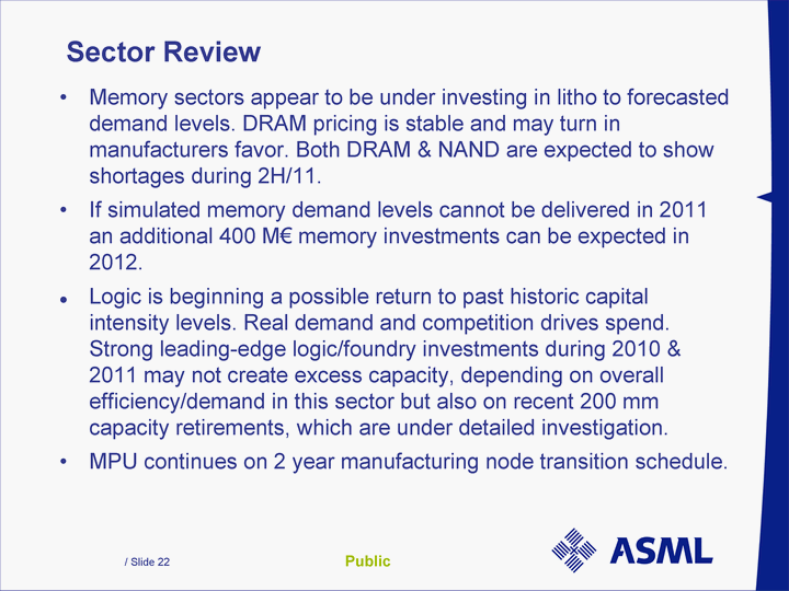
| Sector Review Memory sectors appear to be under investing in litho to forecasted demand levels. DRAM pricing is stable and may turn in manufacturers favor. Both DRAM & NAND are expected to show shortages during 2H/11. If simulated memory demand levels cannot be delivered in 2011 an additional 400 M€ memory investments can be expected in 2012. Logic is beginning a possible return to past historic capital intensity levels. Real demand and competition drives spend. Strong leading-edge logic/foundry investments during 2010 & 2011 may not create excess capacity, depending on overall efficiency/demand in this sector but also on recent 200 mm capacity retirements, which are under detailed investigation. MPU continues on 2 year manufacturing node transition schedule. |
| Products/Technology |
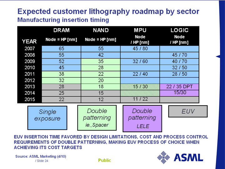
| Expected customer lithography roadmap by sector Manufacturing insertion timing EUV Single exposure Double patterning ie.,Spacer Double patterning LELE Source: ASML Marketing (4/10) EUV INSERTION TIME FAVORED BY DESIGN LIMITATIONS, COST AND PROCESS CONTROL REQUIREMENTS OF DOUBLE PATTERNING, MAKING EUV PROCESS OF CHOICE WHEN ACHIEVING ITS COST TARGETS 15/30 |
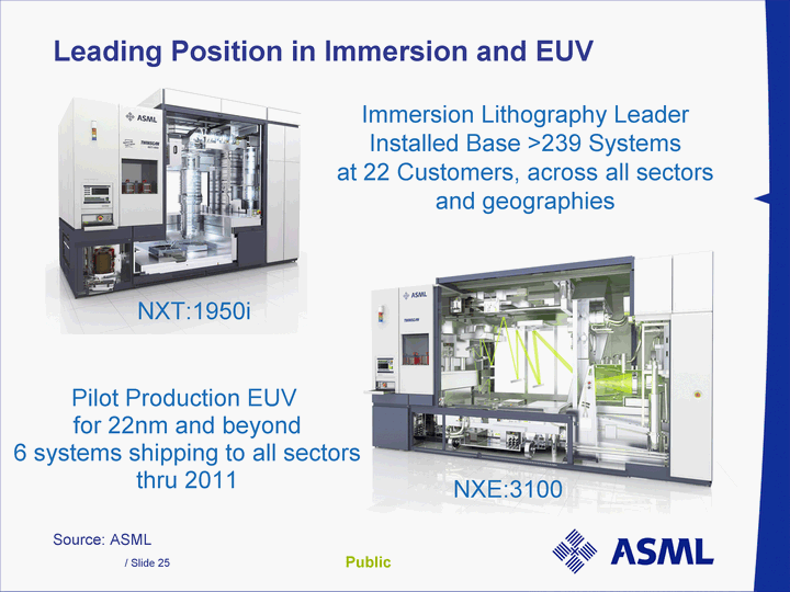
| Leading Position in Immersion and EUV Source: ASML Immersion Lithography Leader Installed Base >239 Systems at 22 Customers, across all sectors and geographies Pilot Production EUV for 22nm and beyond 6 systems shipping to all sectors thru 2011 NXT:1950i NXE:3100 |
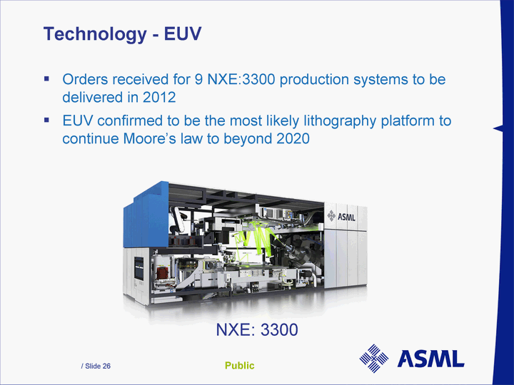
| Technology - EUV Orders received for 9 NXE:3300 production systems to be delivered in 2012 EUV confirmed to be the most likely lithography platform to continue Moore's law to beyond 2020 NXE: 3300 |
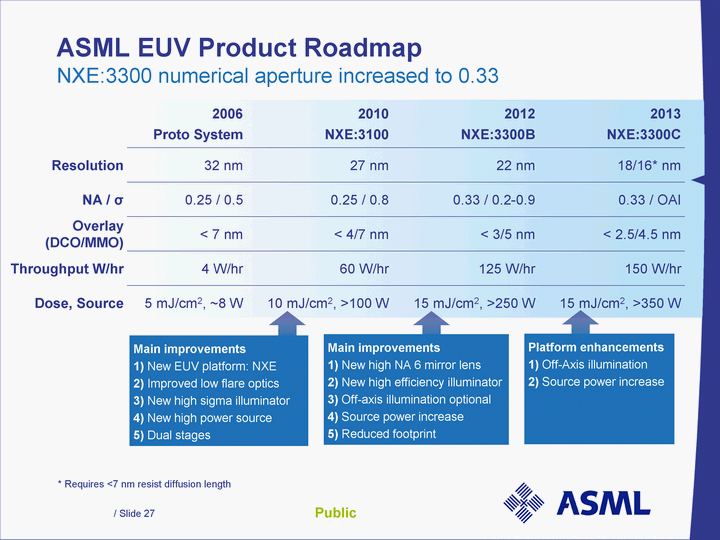
| ASML EUV Product Roadmap NXE:3300 numerical aperture increased to 0.33 * Requires <7 nm resist diffusion length 2006 2010 2012 2013 Proto System NXE:3100 NXE:3300B NXE:3300C Resolution 32 nm 27 nm 22 nm 18/16* nm NA / ^ 0.25 / 0.5 0.25 / 0.8 0.33 / 0.2-0.9 0.33 / OAI Overlay (DCO/MMO) < 7 nm < 4/7 nm < 3/5 nm < 2.5/4.5 nm Throughput W/hr 4 W/hr 60 W/hr 125 W/hr 150 W/hr Dose, Source 5 mJ/cm2, ~8 W 10 mJ/cm2, >100 W 15 mJ/cm2, >250 W 15 mJ/cm2, >350 W Main improvements 1) New EUV platform: NXE 2) Improved low flare optics 3) New high sigma illuminator 4) New high power source 5) Dual stages Main improvements 1) New high NA 6 mirror lens 2) New high efficiency illuminator 3) Off-axis illumination optional 4) Source power increase 5) Reduced footprint Platform enhancements 1) Off-Axis illumination 2) Source power increase |
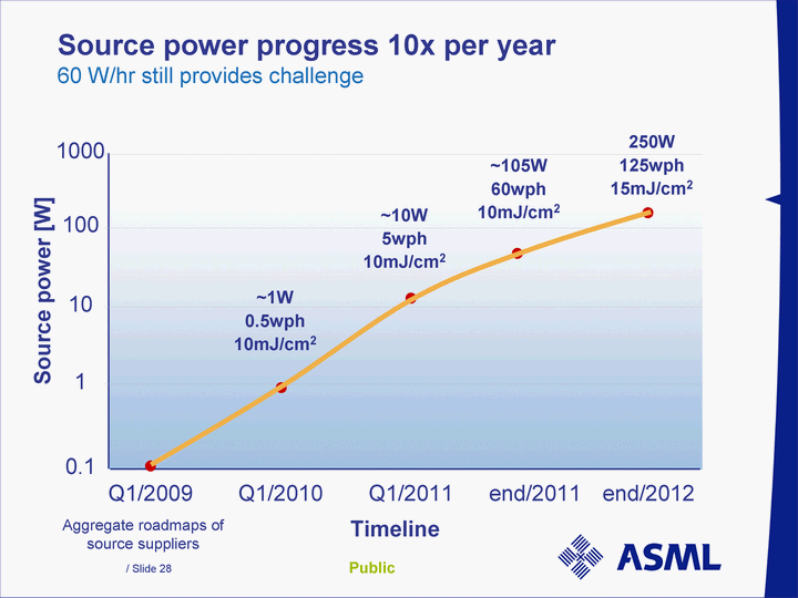
| Source power progress 10x per year 60 W/hr still provides challenge Timeline 0.1 1 10 100 1000 Q1/2009 Q1/2010 Q1/2011 end/2012 250W 125wph 15mJ/cm2 ~10W 5wph 10mJ/cm2 ~1W 0.5wph 10mJ/cm2 end/2011 ~105W 60wph 10mJ/cm2 Source power [W] Aggregate roadmaps of source suppliers |
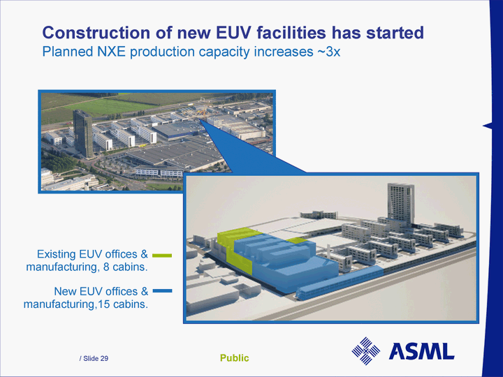
| Existing EUV offices & manufacturing, 8 cabins. New EUV offices & manufacturing,15 cabins. Construction of new EUV facilities has started Planned NXE production capacity increases ~3x |
| EUV is moving forward ASML has 4 years of accumulated EUV field experience with 1st generation EUV tools at research institutes in Belgium and the US 2nd generation EUV NXE:3100 system shipment in progress, 1 system installed and used on customer production site 1 system in installation, 4 additional systems to ship the next half year 3th generation EUV tool NXE:3300 in development, capable of printing features down to 16 nm in volume manufacturing ASML has customer commitments for 10 NXE:3300 systems to be delivered starting in 2012 To meet future EUV demand, construction on the new EUV factory extension has started Productivity roadmap remains significant challenge although major progress continued to be made by 3 source suppliers |
| ASML Strategy and Focus Continue the large R&D outlay to ensure leadership through high product differentiation and provide customers with enabling technologies Improve profitability further by: Improving product mix towards value added software support tools Keeping fixed cost structure to a low break even point, while growing top line Improving further operational performance, by reducing cycle times further, improving its yield and developing even stronger supplier partnerships Continue to returning cash to investors through our existing dividend policy and current excess cash return program Execute on revenue growth trajectory available to ASML in Semiconductor Lithography, and keep reviewing synergistic developments outside Semiconductors for potential limited investments |
