Exhibit 99.1
Marcel Kemp
Director Investor Relations—Europe
DB 2014 TMT Conference
London
September 4, 2014
Forward looking statements
Public
Slide 2 Sep 4, 2014
This document contains statements relating to certain projections and business trends that are forward-looking, including statements with respect to our outlook, expected customer demand in specified market segments, expected sales levels, systems backlog, IC unit demand, expected financial results, gross margin and expenses, expected shipment of tools, productivity of our tools, the development of EUV technology and the number of EUV systems expected to be shipped and timing of shipments, dividend policy and intention to repurchase shares. You can generally identify these statements by the use of words like “may”, “will”, “could”, “should”, “project”, “believe”, “anticipate”, “expect”, “plan”, “estimate”, “forecast”, “potential”, “intend”, “continue” and variations of these words or comparable words. These statements are not historical facts, but rather are based on current expectations, estimates, assumptions and projections about the business and our future financial results and readers should not place undue reliance on them. Forward-looking statements do not guarantee future performance and involve risks and uncertainties. Actual results may differ materially from projected results as a result of certain risks and uncertainties. These risks and uncertainties include, without limitation, economic conditions, product demand and semiconductor equipment industry capacity, worldwide demand and manufacturing capacity utilization for semiconductors (the principal product of our customer base), including the impact of general economic conditions on consumer confidence and demand for our customers’ products, competitive products and pricing, the impact of manufacturing efficiencies and capacity constraints, the continuing success of technology advances and the related pace of new product development and customer acceptance of new products, the number and timing of EUV systems expected to be shipped, our ability to enforce patents and protect intellectual property rights, the risk of intellectual property litigation, availability of raw materials and critical manufacturing equipment, trade environment, changes in exchange rates, available cash, distributable reserves for dividend payments and share repurchases, and other risks indicated in the risk factors included in ASML’s Annual Report on Form 20-F and other filings with the US Securities and Exchange Commission. These forward-looking statements are made only as of the date of this document. We do not undertake to update or revise the forward-looking statements, whether as a result of new information, future events or otherwise.
Content
Public
Slide 3 Sep 4, 2014
| • | | Semiconductor environment |
| • | | Our response: the lithography roadmap |
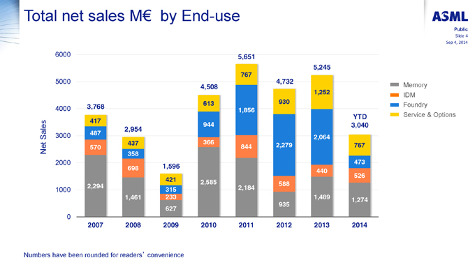
Total net sales M€ by End-use
Public
Slide 4 Sep 4, 2014
6000 5,651
5,245
767
5000 4,732
4,508 Memory
1,252 IDM 613 930
3,768 Foundry
4000 1,856 Service & Options
YTD
417
944 3,040 2,954
3000 487
Sales 2,064
437 366 2,279 767 Net 570 844 358
2000 473
698 1,596
440
526 421 2,585 2,294 588 1000 315 2,184 1,461 233 1,489 1,274 935 627
0
2007 2008 2009 2010 2011 2012 2013 2014
Numbers have been rounded for readers’ convenience
Business environment
Public
Slide 5 Sep 4, 2014
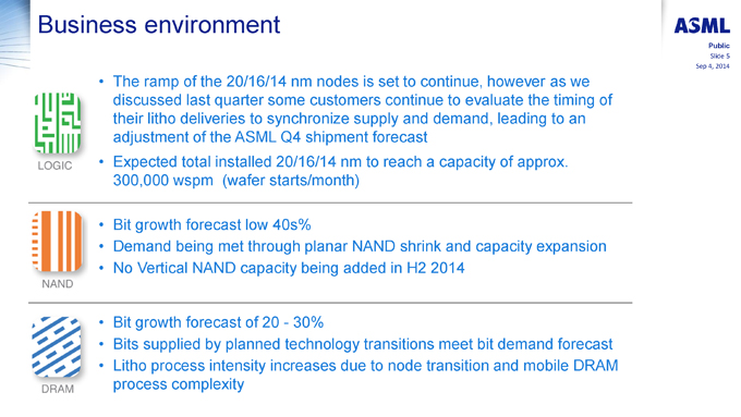
| | • | | The ramp of the 20/16/14 nm nodes is set to continue, however as we discussed last quarter some customers continue to evaluate the timing of their litho deliveries to synchronize supply and demand, leading to an adjustment of the ASML Q4 shipment forecast |
| | • | | Expected total installed 20/16/14 nm to reach a capacity of approx. 300,000 wspm (wafer starts/month) |
| | • | | Bit growth forecast low 40s% |
| | • | | Demand being met through planar NAND shrink and capacity expansion |
| | • | | No Vertical NAND capacity being added in H2 2014 |
| | • | | Bit growth forecast of 20—30% |
| | • | | Bits supplied by planned technology transitions meet bit demand forecast |
| | • | | Litho process intensity increases due to node transition and mobile DRAM process complexity |
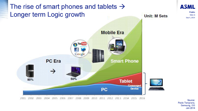
The rise of smart phones and tablets ?
Public
Longer term Logic growth Slide 6 Sep 4, 2014
Source: Pablo Temprano, Samsung, ISS
Jan 2014
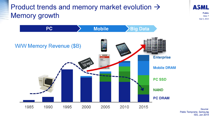
Product trends and memory market evolution ?
Public
Memory growth Slide 7
Diversification in the memory market Sep 4, 2014
PC Mobile Big Data
W/W Memory Revenue ($B)
Enterprise Mobile DRAM
PC SSD
NAND
PC DRAM
1985 1990 1995 2000 2005 2010 2015 Source: Pablo Temprano, Samsung ISS, Jan 2014
Content Public
Slide 8 Sep 4, 2014
| • | | Semiconductor environment |
| • | | Our response: the lithography roadmap |
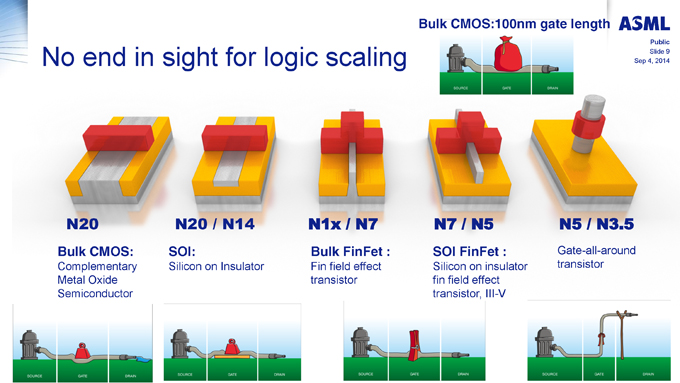
Bulk CMOS:100nm gate length
Public
Slide 9
No end in sight for logic scaling Sep 4, 2014
N20 N20 / N14 N1x / N7 N7 / N5 N5 / N3.5
Bulk CMOS: SOI: Bulk FinFet : SOI FinFet : Gate-all-around
Complementary Silicon on Insulator Fin field effect Silicon on insulator transistor Metal Oxide transistor fin field effect Semiconductor transistor, III-V
Content Public Slide 10 Sep 4, 2014
| • | | Semiconductor environment |
| • | | Our response: the litho roadmap |
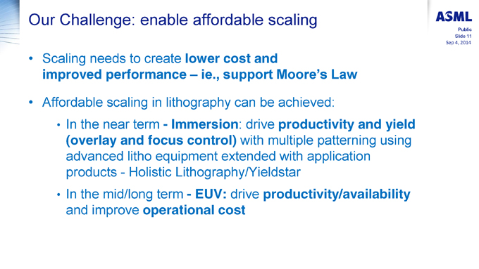
Our Challenge: enable affordable scaling
Public
Slide 11
Sep 4, 2014
• Scaling needs to create lower cost and improved performance – ie., support Moore’s Law
| • | | Affordable scaling in lithography can be achieved: |
| | • | | In the near term - Immersion: drive productivity and yield (overlay and focus control) with multiple patterning using advanced litho equipment extended with application products—Holistic Lithography/Yieldstar |
• In the mid/long term - EUV: drive productivity/availability and improve operational cost
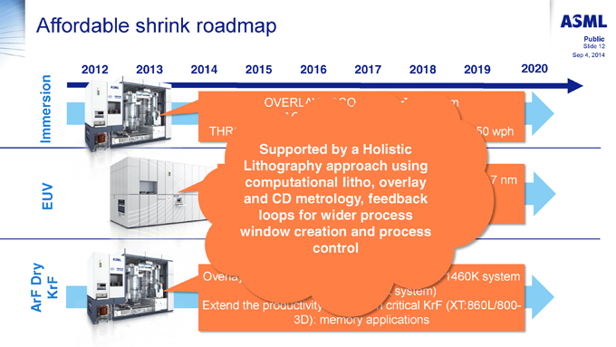
Affordable shrink roadmap
Public
Slide 12 Sep 4, 2014
2012 2013 2014 2015 2016 2017 2018 2019 2020
Immersion ph Supported by a Holistic Lithography approach using computational litho, overlay nm EUV and CD metrology, feedback loops for wider process window creation and process control Dry tem KrF
ArF 800-
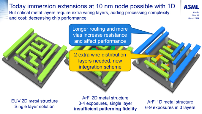
Today immersion extensions at 10 nm node possible with 1D
But critical metal layers require extra wiring layers, adding processing complexity Public
Slide 13
and cost; decreasing chip performance Sep 4, 2014
Longer routing and more vias increase resistance and affect performance
| 2 | extra wire distribution layers needed, new integration scheme |
ArFi 2D metal structure EUV 2D metal structure ArFi 1D metal structure 3-4 exposures, single layer Single layer solution 6-9 exposures in 3 layers insufficient patterning fidelity
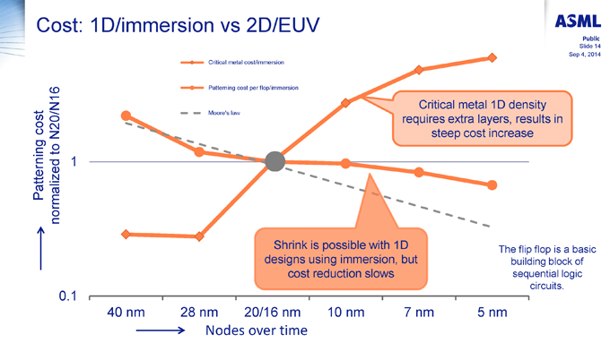
Cost: 1D/immersion vs 2D/EUV
Public
Slide 14 Sep 4, 2014 Critical metal cost/immersion
Patterning cost per flop/immersion
Critical metal 1D density
Moore’s law
cost requires extra layers, results in steep cost increase
N20/N16 to Patterning normalized 1
Shrink is possible with 1D The flip flop is a basic designs using immersion, but building block of cost reduction slows sequential logic
circuits.
0.1
40 nm 28 nm 20/16 nm 10 nm 7 nm 5 nm
Nodes over time
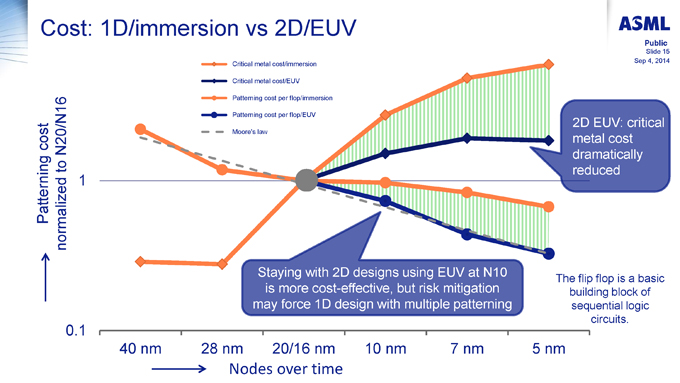
Cost: 1D/immersion vs 2D/EUV
Public
Slide 15 Sep 4, 2014 Critical metal cost/immersion
Critical metal cost/EUV
Patterning cost per flop/immersion
Patterning cost per flop/EUV
2D EUV: critical
Moore’s law
cost metal cost N20/N16 dramatically to reduced
Patterning normalized 1
Staying with 2D designs using EUV at N10
The flip flop is a basic
is more cost-effective, but risk mitigation building block of may force 1D design with multiple patterning sequential logic
circuits.
0.1
40 nm 28 nm 20/16 nm 10 nm 7 nm 5 nm
Nodes over time
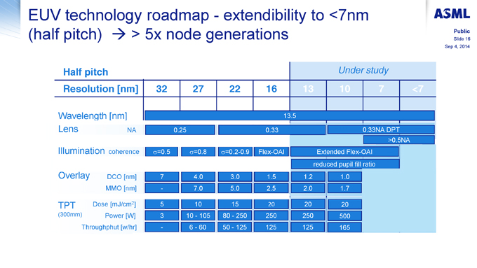
EUV technology roadmap—extendibility to <7nm
(half pitch) ? > 5x node generations Public
Slide 16 Sep 4, 2014
Half pitch Under study
Resolution [nm] 32 27 22 16 13 10 7 <7
layo
Wavelength [nm] 13.5
Lens NA 0.25 0.33 0.33NA DPT >0.5NA Illumination coherence ????5 ????8 ????2-0.9 Flex-OAI Extended Flex-OAI reduced pupil fill ratio Overlay DCO [nm] 7 4.0 3.0 1.5 1.2 1.0 MMO [nm]—7.0 5.0 2.5 2.0 1.7
TPT Dose [mJ/cm2] 5 10 15 20 20 20 (300mm) Power [W] 3 10—105 80—250 250 250 500 Throughphut [w/hr]—6—60 50—125 125 125 165
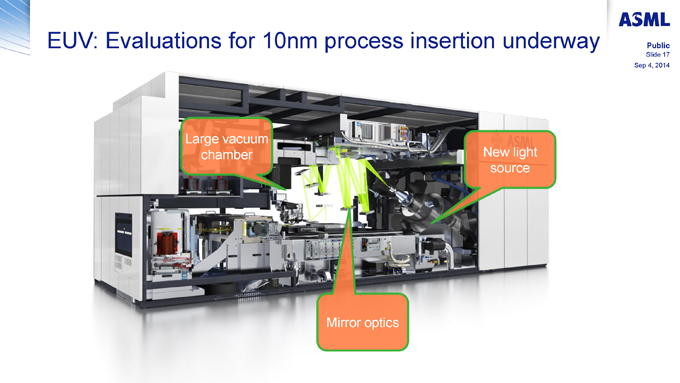
EUV: Evaluations for 10nm process insertion underway Public
Slide 17 Sep 4, 2014
Large vacuum chamber New light source
Mirror optics
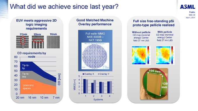
What did we achieve since last year?
Public
Slide 18 Sep 4, 2014
EUV meets aggressive 2D Good Matched Machine Full size free-standing pSi logic imaging Overlay performance proto-type pellicle realized requirements
Without pellicle With pellicle
31nm 22nm 16nm Full wafer MMO
NXE:3300B – CD map (nominal CD map (nominal energy) Center energy) Center NXT:1950i field 27 nm L&S field 27 nm L&S
MMO S2F Stepper Filtered Machine 3
CD requirements by 80 node
70
Tip-to-
60 10 nm x: 99.7% 3.4 nm tip y: 3.3 nm
50
Tip-to- Overlay X Overlay Y
40 line 5
[nm] 4
30
CD 3
20 Lines and
10 spaces MMO[nm]
0 0
20 nm 16 nm 10 nm 7 nm
Systems
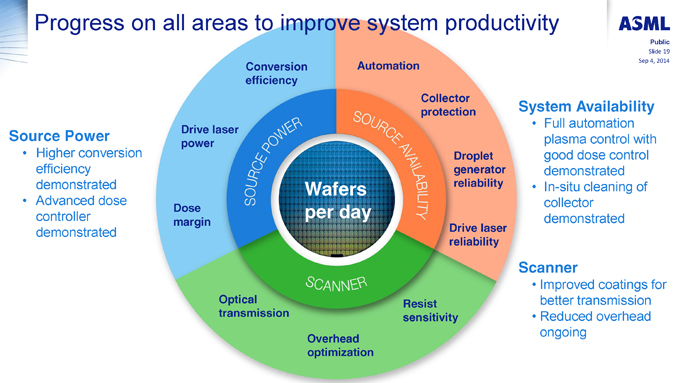
Progress on all areas to improve system productivity
Public
Slide 19
Automation Sep 4, 2014 Conversion efficiency Collector
protection System Availability
Source Power Drive laser power plasma control with
| | • | | Higher conversion Droplet good dose control efficiency generator demonstrated demonstrated Wafers reliability In-situ cleaning of |
| | • | | Advanced dose collector |
Dose per day
controller margin demonstrated demonstrated Drive laser
reliability
Scanner
| | • | | Improved coatings for Optical Resist better transmission |
transmission sensitivity • Reduced overhead
ongoing
Overhead optimization
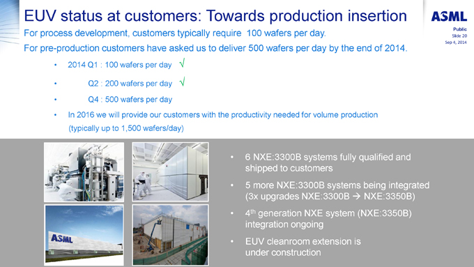
EUV status at customers: Towards production insertion
For process development, customers typically require 100 wafers per day. Public
Slide 20 Sep 4, 2014
For pre-production customers have asked us to deliver 500 wafers per day by the end of 2014.
• 2014 Q1 : 100 wafers per day ?
| | • | | Q2 : 200 wafers per day ? |
| | • | | Q4 : 500 wafers per day |
| | • | | In 2016 we will provide our customers with the productivity needed for volume production (typically up to 1,500 wafers/day) |
| • | 6 NXE:3300B systems fully qualified and shipped to customers |
| | • | | 5 more NXE:3300B systems being integrated (3x upgrades NXE:3300B ? NXE:3350B) |
| | • | | 4th generation NXE system (NXE:3350B) integration ongoing |
| | • | | EUV cleanroom extension is under construction |
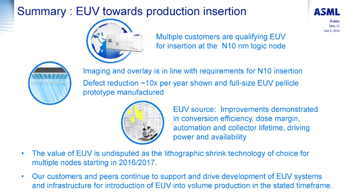
Summary : EUV towards production insertion
Public
Slide 21 Sep 4, 2014
Multiple customers are qualifying EUV for insertion at the N10 nm logic node
Imaging and overlay is in line with requirements for N10 insertion Defect reduction ~10x per year shown and full-size EUV pellicle prototype manufactured
EUV source: Improvements demonstrated in conversion efficiency, dose margin, automation and collector lifetime, driving power and availability
| • | | The value of EUV is undisputed as the lithographic shrink technology of choice for multiple nodes starting in 2016/2017. |
| • | | Our customers and peers continue to support and drive development of EUV systems and infrastructure for introduction of EUV into volume production in the stated timeframe. |

[Graphic Appears Here]