Exhibti 99.1
| Deutsche Bank conference Franki D'Hoore - Director of European Investor Relations London 10 September, 2009 |
| Safe Harbor "Safe Harbor" Statement under the US Private Securities Litigation Reform Act of 1995: the matters discussed in this document may include forward-looking statements, including statements made about our outlook, realization of backlog, IC unit demand, financial results, average sales price, gross margin and expenses. These forward looking statements are subject to risks and uncertainties including, but not limited to: economic conditions, product demand and semiconductor equipment industry capacity, worldwide demand and manufacturing capacity utilization for semiconductors (the principal product of our customer base), including the impact of credit market deterioration on consumer confidence and demand for our customers' products, competitive products and pricing, manufacturing efficiencies, new product development and customer acceptance of new products, ability to enforce patents and protect intellectual property rights, the outcome of intellectual property litigation, availability of raw materials and critical manufacturing equipment, trade environment, changes in exchange rates and other risks indicated in the risk factors included in ASML's Annual Report on Form 20-F and other filings with the US Securities and Exchange Commission. |

| Business update |
| Current rationale of investing in lithography Shrinking of chip designs to lower cost per chip Technology conversions for introduction of new device architectures (e.g. DDR2 to DDR3) Expansion of semiconductor production capacity in leading edge at foundries to enable new applications at lower cost |
| Semiconductor industry indicators are improving Semiconductor unit sales increases since Q1 2009 PC sales higher than previously forecasted Memory prices improving Semiconductor inventory levels well under control Growth drivers in 2010 in consumer products are expected to be personal computers and mobile phones consuming advanced semiconductor chips |
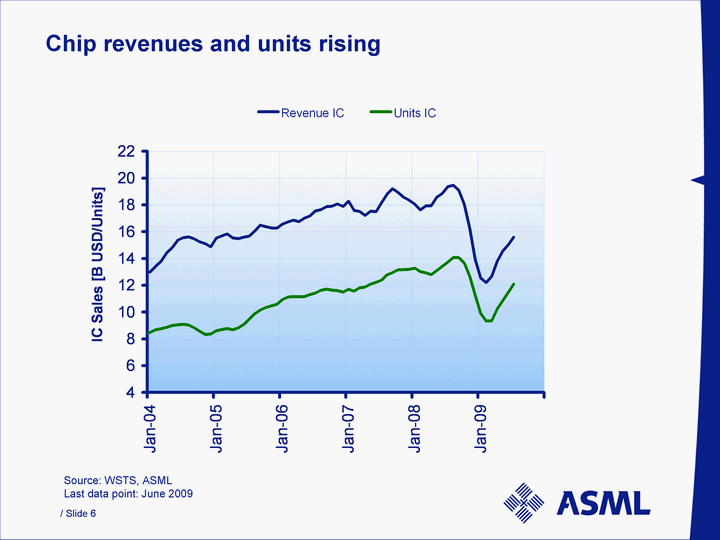
| Chip revenues and units rising Source: WSTS, ASML Last data point: June 2009 |
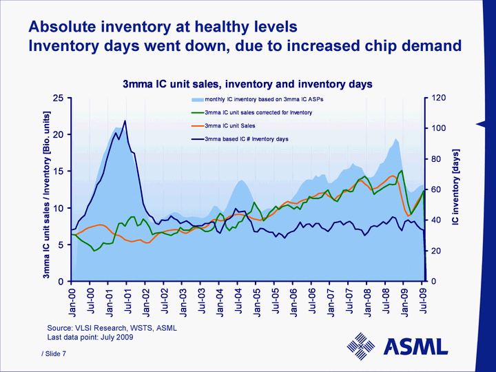
| Absolute inventory at healthy levels Inventory days went down, due to increased chip demand Source: VLSI Research, WSTS, ASML Last data point: July 2009 |
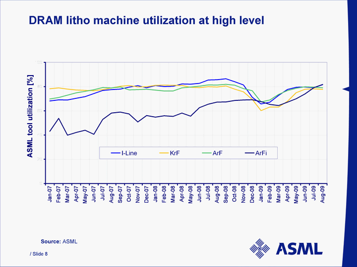
| DRAM litho machine utilization at high level 200 mm tool retirement Steady phase Source: ASML |
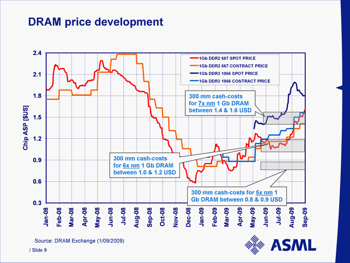
| Source: DRAM Exchange (1/09/2009) DRAM price development 300 mm cash-costs for 5x nm 1 Gb DRAM between 0.8 & 0.9 USD 300 mm cash-costs for 7x nm 1 Gb DRAM between 1.4 & 1.6 USD 300 mm cash-costs for 6x nm 1 Gb DRAM between 1.0 & 1.2 USD |
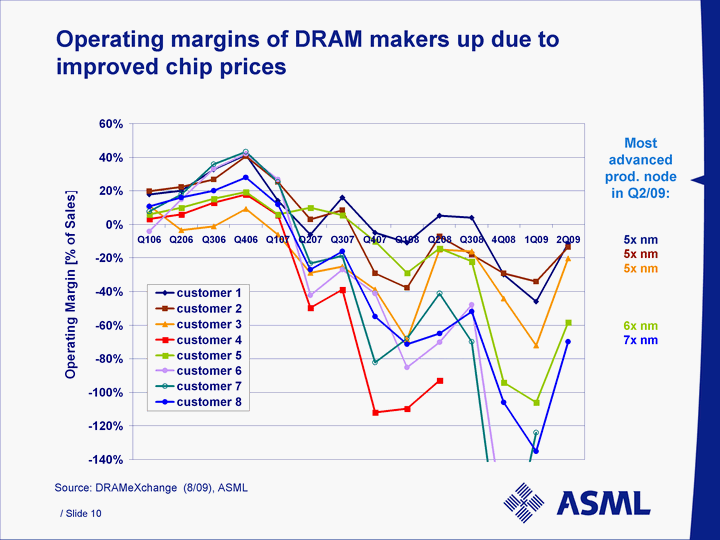
| Operating margins of DRAM makers up due to improved chip prices Source: DRAMeXchange (8/09), ASML Most advanced prod. node in Q2/09: 5x nm 5x nm 5x nm 6x nm 7x nm |
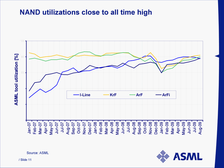
| NAND utilizations close to all time high Source: ASML |
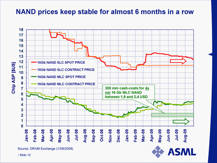
| Source: DRAM Exchange (1/09/2009) 300 mm cash-costs for 4x nm 16 Gb MLC NAND between 1,9 and 2,4 USD NAND prices keep stable for almost 6 months in a row |
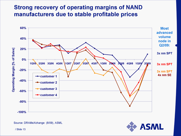
| Strong recovery of operating margins of NAND manufacturers due to stable profitable prices Most advanced volume node in Q2/09: 3x nm SPT 3x nm SPT 3x nm SPT 4x nm SE Source: DRAMeXchange (8/09), ASML |
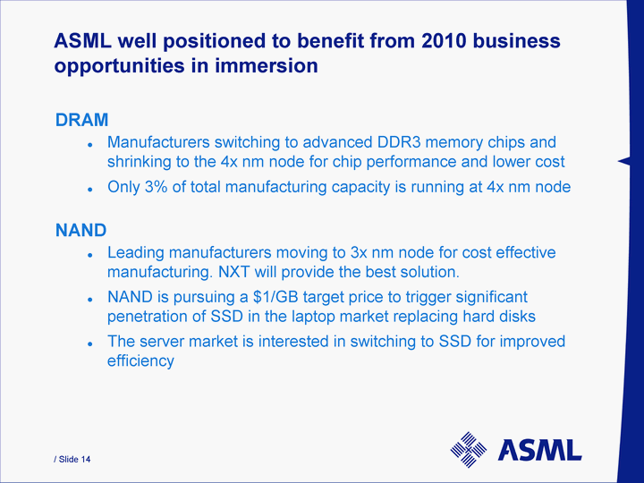
| ASML well positioned to benefit from 2010 business opportunities in immersion DRAM Manufacturers switching to advanced DDR3 memory chips and shrinking to the 4x nm node for chip performance and lower cost Only 3% of total manufacturing capacity is running at 4x nm node NAND Leading manufacturers moving to 3x nm node for cost effective manufacturing. NXT will provide the best solution. NAND is pursuing a $1/GB target price to trigger significant penetration of SSD in the laptop market replacing hard disks The server market is interested in switching to SSD for improved efficiency |
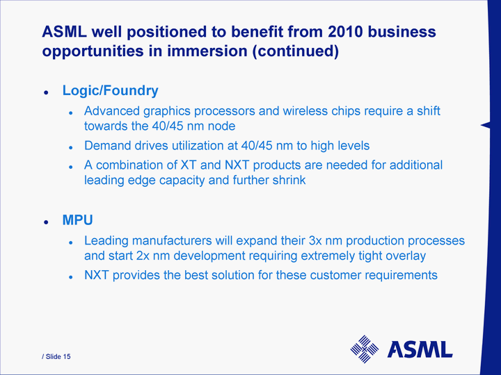
| ASML well positioned to benefit from 2010 business opportunities in immersion (continued) Logic/Foundry Advanced graphics processors and wireless chips require a shift towards the 40/45 nm node Demand drives utilization at 40/45 nm to high levels A combination of XT and NXT products are needed for additional leading edge capacity and further shrink MPU Leading manufacturers will expand their 3x nm production processes and start 2x nm development requiring extremely tight overlay NXT provides the best solution for these customer requirements |
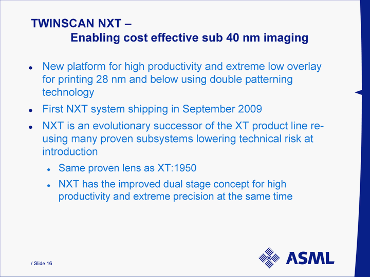
| TWINSCAN NXT - Enabling cost effective sub 40 nm imaging New platform for high productivity and extreme low overlay for printing 28 nm and below using double patterning technology First NXT system shipping in September 2009 NXT is an evolutionary successor of the XT product line re- using many proven subsystems lowering technical risk at introduction Same proven lens as XT:1950 NXT has the improved dual stage concept for high productivity and extreme precision at the same time |
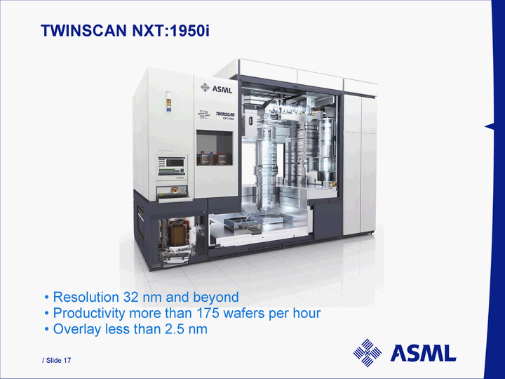
| Resolution 32 nm and beyond Productivity more than 175 wafers per hour Overlay less than 2.5 nm TWINSCAN NXT:1950i |
| Summary ASML used previous quarters with low sales volume to: Increase technological leadership EUV, NXT double patterning, holistic lithography Work on cost improvements Reduce manufacturing cycle time ASML new products XT:1950 and NXT:1950 will enable all technology transitions needed to support: 4x nm DDR3 DRAM business 4x nm shrink in foundry 3x nm NAND manufacturing 2x microprocessor development |
| Commitment |