Shrink, an expanding
(litho) market
Martin van den Brink
Executive Vice President
Marketing and Technology
ISS, Half Moon Bay, Jan 9, 2007
Immersion
EUV
Content
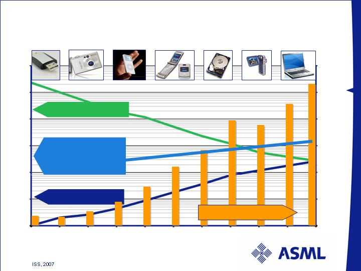
The demand for shrink continues
Litho roadmap
Litho integration
Litho cost
Summary
/ Slide 2
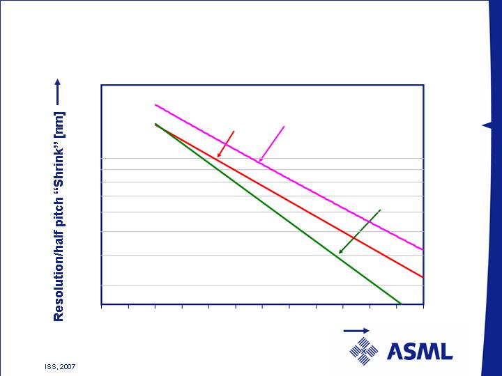
Shrink rates for Logic, DRAM, and NAND flash
Source: Various customers, dates determine production start/qualification
Year
10
12
200
100
80
60
40
Logic
11
07
09
08
04
06
05
01
03
02
00
NAND
DRAM
/ Slide 3

Shrink
Shrink speed is defined using “half pitch”
Half pitch is led by Flash with k factors below 0.30
DRAM is trailing Flash by about 10%
Logic and µP are trailing Flash by about 50%
Logic customers use “node” instead of “half pitch”
On average, the relation is 70% “half pitch” = ”node”
/ Slide 4
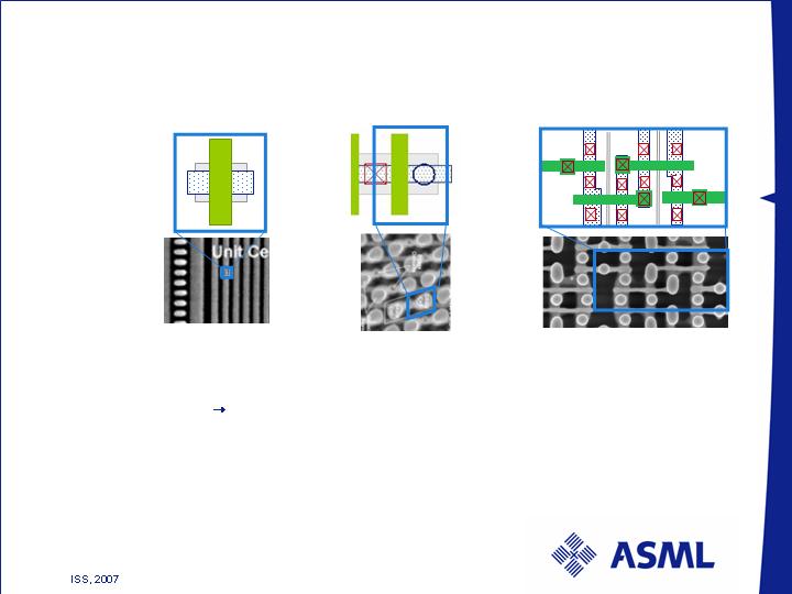
IC characteristics & Lithography implications
NAND Flash
X-point storage
transistor
4 F2
1 4
1D
Dense
Resolution
Strong
0.27 ~ 0.29
DRAM
Transistor
+ Capacitor
6~8 F2
1
1D & 2D
Dense
Imaging & overlay
Moderate
0.29 ~ 0.31
Cell
layout
Logic / SRAM
6 Transistor (SRAM)
50~60 F2
1
2D
Random
OPC, DoF
Weak
0.36 ~ 0.38
Device:
Typical Cell Size:
Bits/cell
Critical Patterns:
Critical Pitch:
Shrink Challenge:
RET:
k 1 limit:
6 Transistor SRAM Cell
Typical
Device
Pattern
/ Slide 5
Shrink drives cost per function and market growth
Source: Gartner Dataquest, iSuppli, ASML
2000
2001
2002
2003
2004
2005
2006
2007
2008
2009
2010
NAND cost, $ / GB
NAND size, GB
0.01
0.10
1.00
10.0
100
1,000
10,000
0
5,000
10,000
15,000
20,000
25,000
30,000
NAND Revenue, M$
Projected cross-
over
HDD - NAND, GB
40-80 GB
1-2 GB
64-150 GB
1 GB
4 GB
8 GB
8-16 GB
Expected memory size sweet-spot:
/ Slide 6
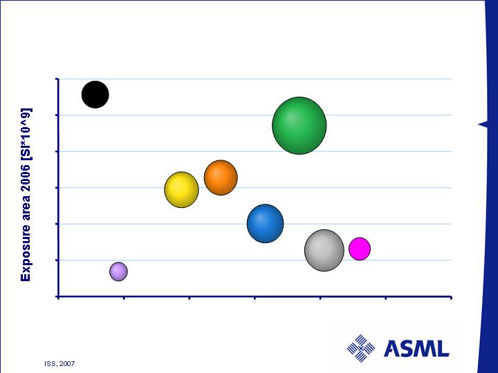
Sources: ASML MCC, VLSI Research, iSuppli, SIA
NAND Flash fastest growing IC segment between
2006 and 2009 in terms of silicon exposure area
DRAM
LOGIC
NAND
NOR
ANALOG
MICRO
Other
0
10
20
30
40
50
60
0
5
10
15
20
25
30
CAGR Exposure Area 06-09 [%]
Segment size:
20 Bio. US$
/ Slide 7

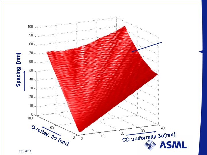
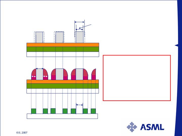
Resolution, CD uniformity & overlay drive shrink
Layout 6 transistor SRAM Cell
Design Rule & Cell Area [m m2]
CD
CD
Spacing
X-section
through Cell
Source: IMEC, TI
Node
Aggressive
Typical
Relaxed
130 nm
2.00
2.50
3.00
90 nm
1.00
1.25
1.50
65 nm
0.45
0.55
0.80
45 nm
0.20
0.27
0.34
32 nm
0.10
0.13
0.19
cell area 0.24 µm2
metal pitch 130nm
ArF immersion
CDU
& Overlay
CDU
& Overlay
/ Slide 8
Overlay and resolution (-control) key for device scaling
Modeled
equal 99.9%
yield plane
/ Slide 9
Content
The demand for shrink continues
Litho roadmap
Dry
Immersion
Double patterning
EUV
Litho integration
Litho cost
Summary
/ Slide 10
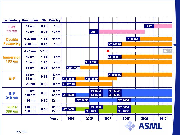
Roadmap scenarios
Resulting k 1 as function of resolution, wavelength and NA
k1 = (half pitch) * NA / wavelength
Most aggressive k1 in production today = 0.3,
physical limit single exposure = 0.25
Practical limit double patterning = 0.2
/ Slide 11
100
65
45
32
22
16
11
year
2005
2007
2009
2011
2013
2015
[nm]
NA
248
0.80
0.32
193
0.93
0.31
1.20
0.40
0.28
1.35
0.31
0.22
0.15
1.55
0.26
0.18
13.5
0.25
0.59
0.41
0.35
0.57
0.41
0.45
0.53
0.37
half pitch
First super high NA immersion system enables 45 nm
/ Slide 12
First super high NA immersion
system enables 45 nm
100
65
45
32
22
16
11
year
2005
2007
2009
2011
2013
2015
[nm]
NA
248
0.80
0.32
193
0.93
0.31
1.20
0.40
0.28
1.35
0.31
0.22
0.15
1.55
0.26
0.18
13.5
0.25
0.59
0.41
0.35
0.57
0.41
0.45
0.53
0.37
half pitch
-300nm
NF
+300nm
+450nm
-500nm
-180nm
+180nm
950nm DoF
-240nm
NF
+120nm
+210nm
-300nm
-120nm
+60nm
500nm DoF
-150nm
NF
+150nm
+210nm
-210nm
-90nm
+90nm
400nm DoF
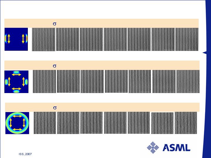
50nm 1.2NA, =0.74/0.94, annular, XY polarization, k1 = 0.31
45nm 1.2NA, =0.82/0.97, C-Quad-30, XY polarization, k1 = 0.28
42nm 1.2NA, =0.89/0.98, Dipole X-35, Y polarization, k1 =0.261
@ 550mm/s Scan speed
Overview dense line 1700i imaging results
/ Slide 13
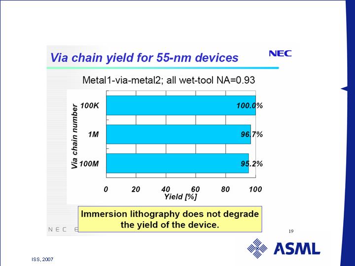
Immersion performance deficiency not impacting yield
Teruhiko Kodama, NEC, Symposium on
Immersion Technology, Kyoto, oct 06
/ Slide 14
Roadmap scenarios, the impact of immersion
Water-based 193 not sufficient for 32-nm half pitch
/ Slide 15
Max NA water-based 193 nm immersion
requires double patterning to get to 32 nm
100
65
45
32
22
16
11
year
2005
2007
2009
2011
2013
2015
[nm]
NA
248
0.80
0.32
193
0.93
0.31
1.20
0.40
0.28
1.35
0.31
0.22
0.15
1.55
0.26
0.18
13.5
0.25
0.59
0.41
0.35
0.57
0.41
0.45
0.53
0.37
half pitch
Single Exposure (like EUV) Litho requirements
Real CD is smaller than target CD
Error caused by litho step
CD error during
litho process
steps will result
in smaller lines
Extra CD errors
are created
during etch step
Combined with
litho CD error to
a Final CD error
Target CDlitho
CD determined by 2
error components
litho and etch:
DCDlitho < 7% of CD
Overlay < 20% of CD
Target CD < 10% CD
/ Slide 16
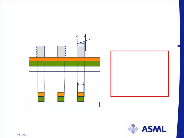
Litho Double Patterning Litho requirements
Real CDlitho is smaller than target
CDlitho
Error caused by litho
Target CDlitho
CD determined by 8
error components; 2 x
litho, 2 x etch and
overlay:
DCDlitho < 3,5% of CD
Overlay < 7% of CD
Final CD < 10% CD
1st Photo CD
errors during
litho will result in
smaller/larger
lines
1st Etch+CD trim
Extra CD errors
could take place
2nd Photo
Overlay error
translates into
CD error
between lines
2nd etch+CD trim
2nd pattern with
CD errors from
2nd etch/trim and
overlay
/ Slide 17
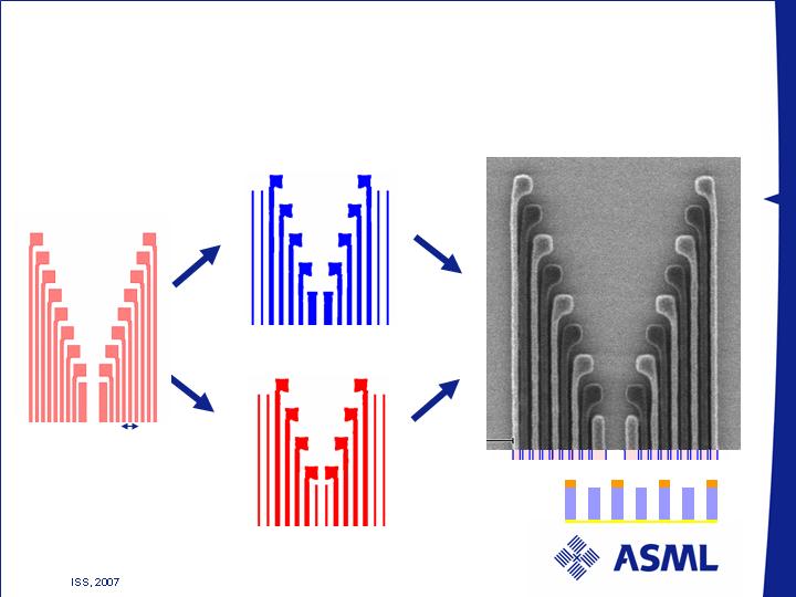
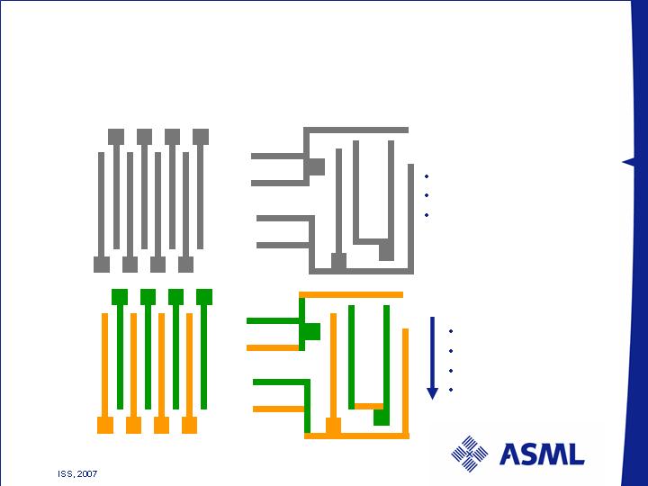
Double line patterning; 32-nm half pitch Flash
MASK A
MASK B
Pitch = 64nm
Target
Min Pitch 64nm
k1 = 0.20
SPLIT + OPC
Poly patterning
Annular 0.8/0.5, X-Y polarized
XT:1700i, 193nm - 1.2NA
Co work ASML, Imec, Synopsys and Mentor Graphics
Hard mask
Poly
/ Slide 18
New software & algorithms required to split &
optimize OPC and stitching for Double Patterning
Memory
Logic
Original
layout
Pattern
split
NAND Flash
DRAM
Restricted Logic
Random Logic
Increasing Difficulty
Challenges
Correct decomposition
OPC for decomposition
Model-based stitching
error compensation
/ Slide 19
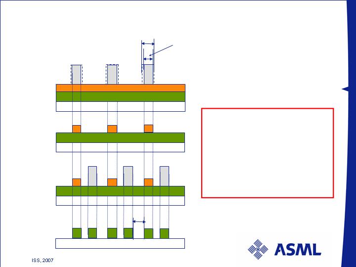
Spacer Double Patterning Litho requirements
Real CD is smaller than target CD
Error caused by litho and etch trim
patterning steps
Sacrificial line
patterning:
A CD error
during litho and
etch process
steps will result
in smaller lines
Line CD error
propagates
during spacer
uniform
deposition and
etched back
Initial CD error
becomes a
pitch variation
on the final
pattern
Target CDlitho
CD determined by 11 error
components; litho, etch,
spacer deposition, trim and
final etch:
DCDlitho < 3 % of CD
Overlay < 20% of CD
Final CD < 10%CD
/ Slide 20
CD and overlay litho budget challenge
3-4
2
1
# process steps relative to
single exposure
2-3
2
1
# mask steps
20%
3%
Spacer
double
patterning
3,5%
7%
CD
7%
20%
Overlay
Litho
double
patterning
Single
exposure
Litho exposure Equipment
parameter as percentage of CD
/ Slide 21
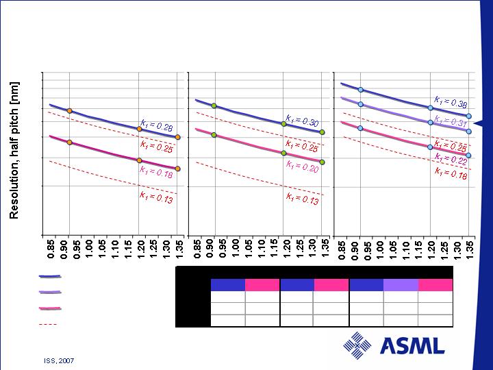
Lithography Limits for ArF Single & Double Patterning
10
100
20
30
40
50
60
80
NAND Flash
Physical limit
Double Patterning limit
Double Exposure limit
Single Exposure limit
DRAM
Logic
NA
SE
DPT
SE
DPT
SE
DE
DPT
0.93
58
37
62
42
80
65
45
1.20
45
29
48
32
60
50
35
1.35
40
26
43
29
55
45
31
NAND
DRAM
Logic
ArF
/ Slide 22
32 nm half pitch with 193 immersion
extremely challenging
/ Slide 23
NA 1.55 requires new liquid, new glass
and very low k1 to extend to 32nm
100
65
45
32
22
16
11
year
2005
2007
2009
2011
2013
2015
[nm]
NA
248
0.80
0.32
193
0.93
0.31
1.20
0.40
0.28
1.35
0.31
0.22
0.15
1.55
0.26
0.18
13.5
0.25
0.59
0.41
0.35
0.57
0.41
0.45
0.53
0.37
half pitch
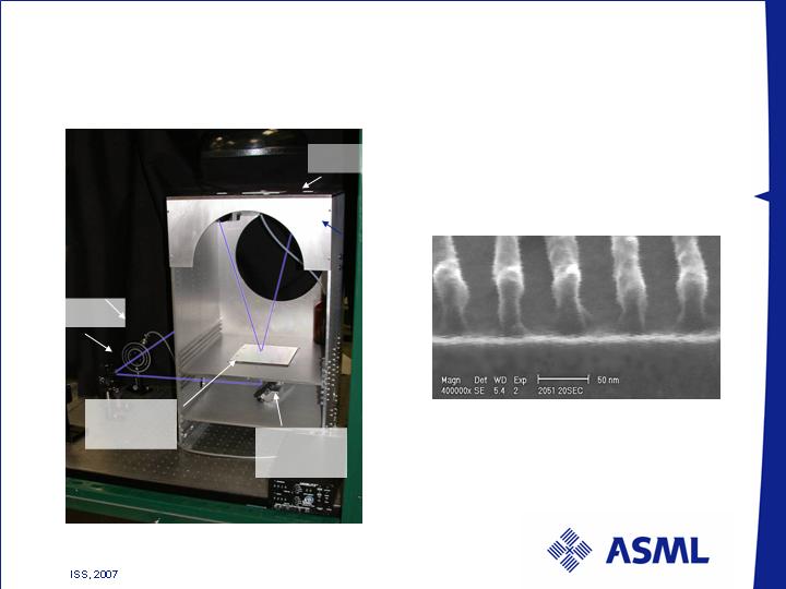
29-nm imaging on interference set-up
Version I Interferometer
85 nm ARC-29A, 50 nm PARIM850 resist
Imaging results with
Dupont IF169
beam
splitter
Fold
mirror
laser
Wafer
/ Slide 24
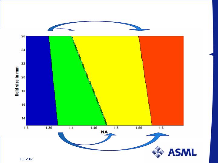
Apertures, field sizes and refractive indices
Water
based
litho
Second gen
fluid
n=1.65
Quartz
lens material
n = 1.57
Second gen fluid
n=1.65
New
lens material
n>1.9
New fluid
n>1.8
New
lens material
n>1.9
New resist
N>1.8
7%
15%
4%
15%
/ Slide 25
Historic reduction stepper imaging technology changes
3.3
29
34
39
48
62
91
109
Diffraction
limit [nm]
15
>2010
> 6
193 nm/HI
1031
>2010
>10
13 nm/ vacuum
44
2006
3
193 nm/water
23
-
Failed
157 nm/air
28
2002
7
193 nm/air
47
1995
9
248 nm/air
19
1989
3
365 nm/air
-
1980
-
436 nm/air
Incremental
Improvement %
Production
Insertion
Incubation
time [yr]
Technology
/ Slide 26
EUV the only high volume opportunity
100
65
45
32
22
16
11
year
2005
2007
2009
2011
2013
2015
[nm]
NA
248
0.80
0.32
193
0.93
0.31
1.20
1.35
0.15
1.55
0.26
0.18
13.5
0.25
0.59
0.41
0.35
0.57
0.41
0.45
0.53
0.37
half pitch
EUV required for 32 nm as cost reduction
for double patterning and more extendable
technology than non water immersion
/ Slide 27
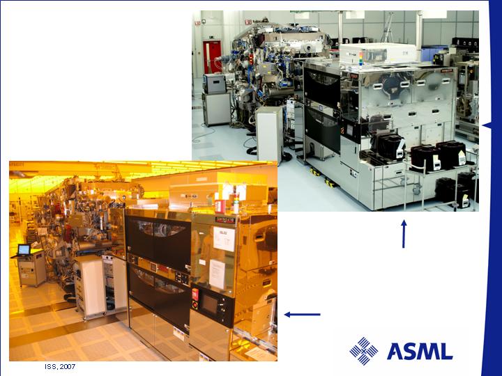
Installation of EUV
in progress
(Dec. 2006)
Albany
Leuven
/ Slide 28
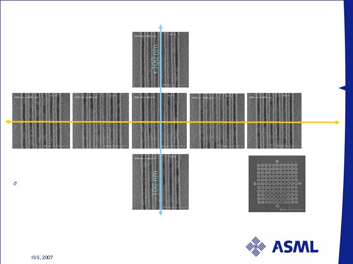
Full field, through focus 40 nm lines, 55 contacts
Resist: MET-2D, ~18 mJ/cm2
NA=0.25
= 0.5 (conventional illumination)
Field point
-10.6 mm
-6.36 mm
6.36 mm
10.6 mm
Focus
/ Slide 29
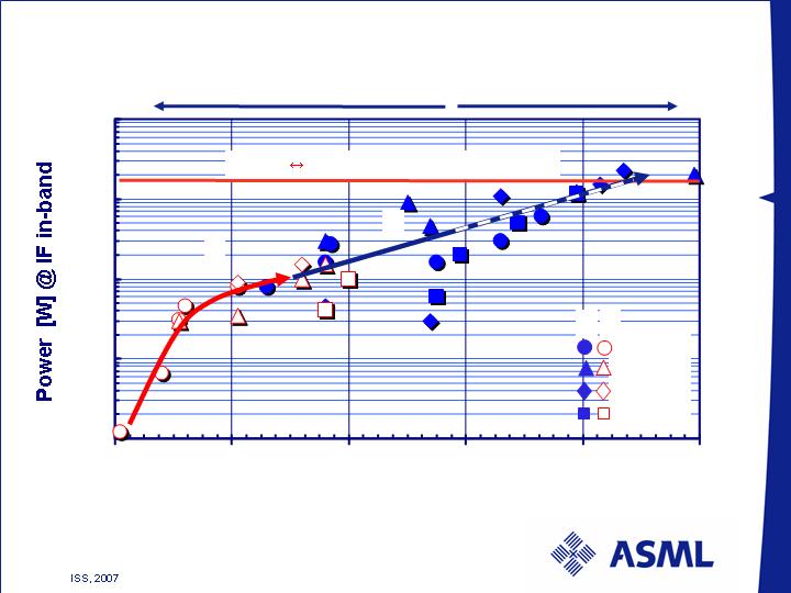
0.1
1
10
100
1000
2001
2003
2005
2007
2009
2011
Year
Planned performance
Source power progress has been increasing
supplier 2
supplier 1
supplier 3
supplier 4
180 W 100 W/hr @ 10 mJ/cm2
Actual data
Sn
Xe
Sn
Xe
/ Slide 30
/ Slide 31
Low k1
challenge
half pitch
0.37
0.53
0.45
0.41
0.57
0.35
0.41
0.59
0.25
13.5
0.18
0.26
1.55
0.15
0.22
0.31
1.35
0.28
0.40
1.20
0.31
0.93
193
0.32
0.80
248
NA
[nm]
2015
2013
2011
2009
2007
2005
year
11
16
22
32
45
65
100
Likely technology roadmap
Pitch relaxation or
Double patterning
Fluid/
material
challenge
Infrastructure challenge
opportunity
likely
ASML 300mm Product Roadmap
High Index decision point
193nm
/ Slide 32

Content
The demand for shrink continues
Litho roadmap
Litho integration
Litho cost
Summary
/ Slide 33
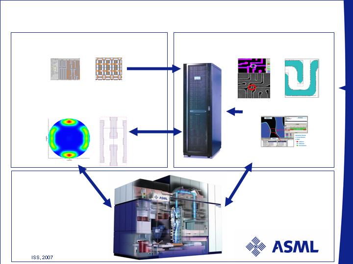
High k1 : Low Design to Wafer Integration
Design & Layout
Mask Shop
High k1 (>0.5) : Independent Design, Mask Manufacture & Wafer Processing
Wafer Fab
/ Slide 34
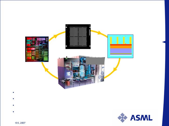
Low k1 : High Design to Wafer Integration
Low k1 (<0.4) : Integration of design, mask and Lithography processes
Litho aware design constrains
Design for
Manufacturing
DFM
Application
Specific
Manufacturing
Design space
Manufacturing space
/ Slide 35
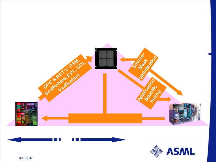
ASML & Brion: Integrated manufacturing solution
Brion
Ultra fast verification & RET/OPC
LithoCruiser: Source & Mask Optimization
Scanner data &
optimization
ASML MaskTools
Reticle Enhancement Technologies
Chrome-less
Phase-shift
technology (CPL)
Scattering Bars
placement
technology
Production Litho
Verification
Production
RET/OPC
Process Window
Coverage
Tachyon
Platform
ASML TWINSCAN
Highest productivity
scanner
Source
definition
/ Slide 36
Extending Lithography is driving Integration of
Design, Mask, Process and Exposure
IC Design
RET
mask
193i
Process
flow
193 Immersion with hyper NA and low k1 capability
IC design for manufacturability, DFM
Source-mask optimization, Litho, RET&OPC
Process flow optimized for low contrast imaging, optimal CD
and stitching (overlay)
/ Slide 37

Content
The demand for shrink continues
Litho roadmap
Litho integration
Litho cost
Summary
/ Slide 38
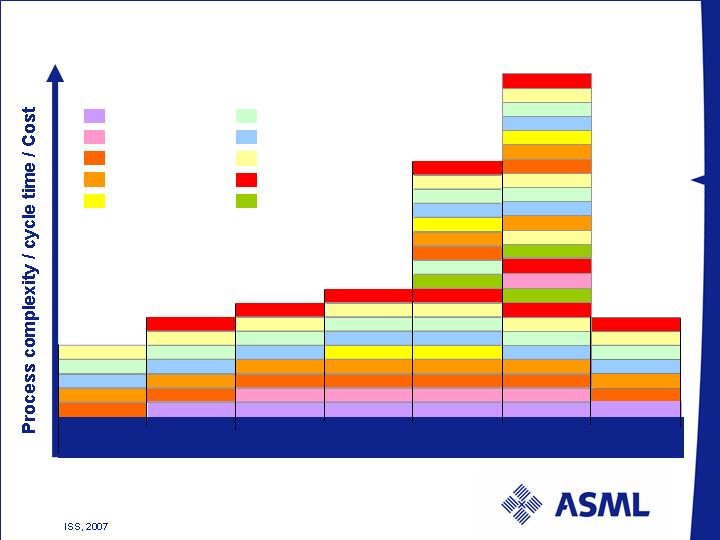
Increased litho process complexity drives cost
Hard Mask Etch
Resist
Organic BARC
Hard Mask
Expose
Develop
Inorganic BARC
Metrology
Strip & Clean
Top Coat
KrF
ArF
ArF
ArFi
ArFi DPT
130nm
90nm
65nm
45nm
32nm
32nm
EUV
32nm
DPT = Double Patterning
Spacer DPT
/ Slide 39
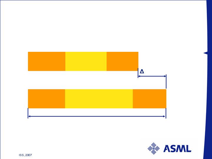
A Process (Single Exposure)
Lithography
Lithography
B Process (Double Exposure)
Cycle time
Cycle time
Higashiki, Tosiba, Santa Clara, SPIE march 06
Cycle time of multiple exposure strategies increases
/ Slide 40
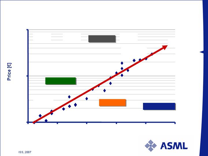
Lithography System Price Evolution
1M
10M
100M
1985
1990
1995
2000
2005
2010
Year
i-line
300mm
200mm
150mm
KrF
ArF
ArFi
EUV
Wafer Size
Wavelength
Stepper
Platform
Step & Scan
Dual Stage
0.4
0.5
0.6
0.7
0.8
0.93
1.2
Aperture
€40M?
/ Slide 41
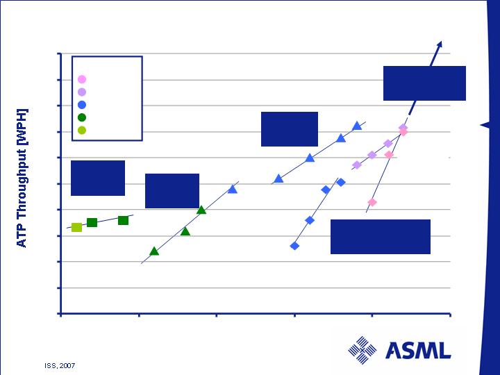
ASML System Throughput Improvement
0
40
80
120
160
200
1985
1990
1995
2000
2005
2010
XT:1450G
g-line
i-line
KrF
ArF
Immersion
Wavelength
Year of Introduction
XT:1400Ei
XT:1700Fi
200mm
Stepper
Future DPT
requirement
150mm
Stepper
200mm
Scanner
TWINSCAN
300mm Scanner
XT:1900Gi
/ Slide 42
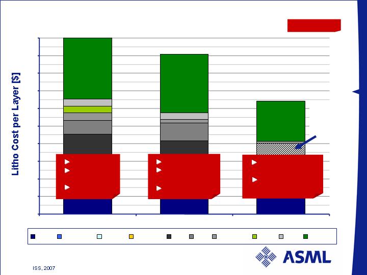
Litho cost per layer: estimates for 32nm
* Mask cost based on 5000 wafers / mask usage
0
20
40
60
80
100
193nm Spacer DPT
193nm Litho DPT
EUV
Fixed
Operating
Source
Chemical
CVD
Etch
Metrology
Other
Strip
Reticle
Defect free mask
/ no pellicle
Source power /
resist sensitivity
Pattern split
Process
complexity
Overlay & CDU
Pattern split
Process
complexity
CDU control
Challenges
Further cost
reduction
opportunity?
/ Slide 43
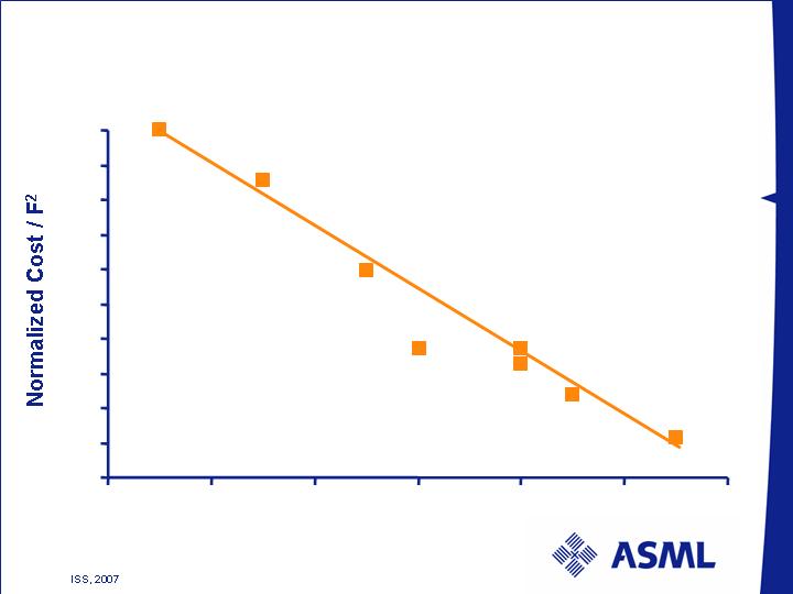
XT:1400
65 nm
0.93 NA ArF
0.0
0.1
0.2
0.3
0.4
0.5
0.6
0.7
0.8
0.9
1.0
2000
2002
2004
2006
2008
2010
2012
Lithography cost affordability:
Cost per minimum Feature2 continuous shrink
32 nm
0.25 NA EUV
(60 WPH)
22 nm
0.25 NA EUV
(100 WPH)
XT:1700i
45 nm
1.2 NA ArFi
AT:850
130 nm
0.8 NA KrF
XT:1250
90 nm
0.85 NA ArF
Source: ASML
32 nm
ArFi DPT
32 nm
Spacer DPT
/ Slide 44

Content
The demand for shrink continues
Litho roadmap
Litho integration
Litho cost
Summary
/ Slide 45
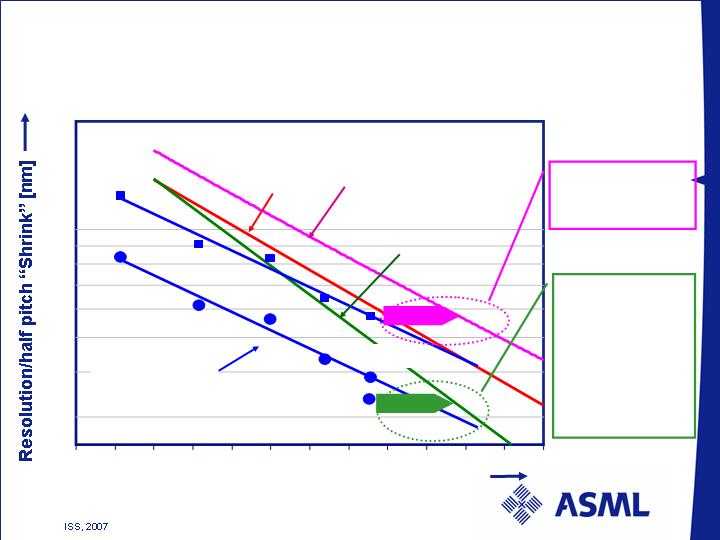
Shrink rates for Logic, DRAM, and NAND flash
versus tool introduction at k1 0.27 and 0.40
Source: Various customers, dates determine production start/qualification
10
12
200
100
80
60
40
11
07
09
08
04
06
05
01
03
02
00
Year
ASML Product
Introduction
XT:1400
XT:1700i
AT:1200
AT:850
XT:1900i
k1=0.4
k1=0.27
Logic
DRAM
R&D
R&D
NAND
To enable
continued
shrink for
memory: EUV is
needed, Double
Patterning to
bridge gap until
EUV mature
Litho technology
will allow Logic
to shrink
XT:1450
Double
Patterning
/ Slide 46

Summary lithography roadmap
Water based immersion will capture the 40 nm half pitch
using 1.35 NA 193 nm lithography.
Non water based immersion needs new lens materials to
increase resolution capability significantly:
New fluid technology advantage for full field resolution limited by
existing lens materials to 4%, not sufficient to give economic return
to equipment supplier and its user.
New lens material technology still needs to mature, this will push
any product implementation beyond 2009.
EUV technology acceptance is significantly growing with
shipments of EUV Alpha Demo Tools and orders for pre-
production tools but is still below industry threshold.
Hence double patterning is the only option in the 2008-2009
time frame. ASML will support this with sufficient overlay
and productivity on their products in time.
/ Slide 47

Summary lithography integration and cost
Extension of 193 nm is requiring tighter CD and overlay,
yielding DPT split and processing. This will drive the
integration of design, mask, process and exposure, resulting in
integrated DFM solutions as well as mask and application
specific manufacturing.
EUV becomes a cost, cycle time and performance
improvement opportunity due to more CD and overlay tolerant
single patterning process and single mask with low OPC
content. However the infrastructure needs to be developed.
EUV introduction will be driven by the need for shrink from
memory manufactures.
The required amount, performance and complexity of
lithography tools, resist, process and mask will go up in any
scenario which should be positive for the integral litho
business (mask, exposure, process and optimization software
tools) however litho cost needs to be addressed by higher
productivity.
/ Slide 48
Commitment