Exhibit 99.4
| Long-Term Lithography Market Potential Dr. Antonio Mesquida Kusters, Director of Market Intelligence London, November 2nd 2007 Investor Day |
| Contents Introduction Long-term market potential (2006 - 2012) ASML's Lithography Demand Simulation Model Some examples of simulated market scenarios Summary & Conclusions |
| Introduction Driven by a relatively stable market since the last down-turn in 2001-02, ASML has increased YoY revenues since then, mainly driven by: Increased CapEx spending, driven by strong memory investments Increased spending share of lithography segment out of total CapEx Increased market share for ASML in almost all sub-segments But, what is expected to happen looking from a mid- to long-term perspective and what are the drivers behind? |
| Contents Introduction Long-term market potential (2006 - 2012) ASML's Lithography Demand Simulation Model Some examples of simulated market scenarios Summary & Conclusions |
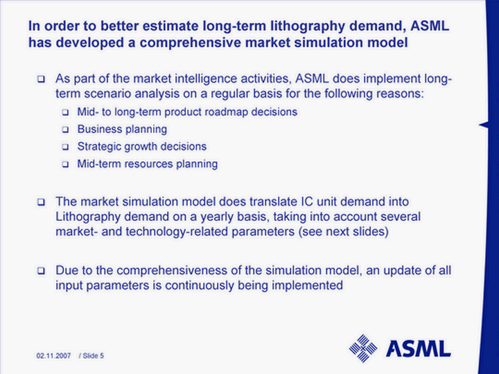
| In order to better estimate long-term lithography demand, ASML has developed a comprehensive market simulation model As part of the market intelligence activities, ASML does implement long- term scenario analysis on a regular basis for the following reasons: Mid- to long-term product roadmap decisions Business planning Strategic growth decisions Mid-term resources planning The market simulation model does translate IC unit demand into Lithography demand on a yearly basis, taking into account several market- and technology-related parameters (see next slides) Due to the comprehensiveness of the simulation model, an update of all input parameters is continuously being implemented |
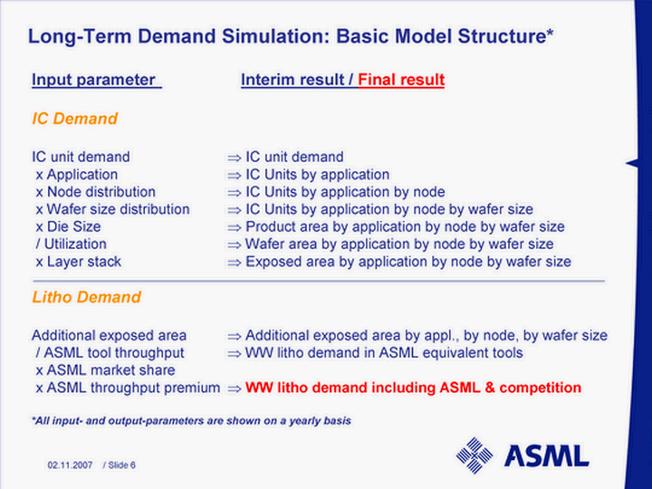
| Long-Term Demand Simulation: Basic Model Structure* Input parameter Interim result / Final result IC Demand IC unit demand ? IC unit demand x Application ? IC Units by application x Node distribution ? IC Units by application by node x Wafer size distribution ? IC Units by application by node by wafer size x Die Size ? Product area by application by node by wafer size / Utilization ? Wafer area by application by node by wafer size x Layer stack ? Exposed area by application by node by wafer size Litho Demand Additional exposed area ? Additional exposed area by appl., by node, by wafer size / ASML tool throughput ? WW litho demand in ASML equivalent tools x ASML market share x ASML throughput premium ? WW litho demand including ASML & competition *All input- and output-parameters are shown on a yearly basis |
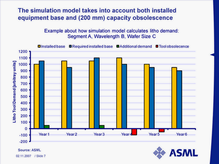
| The simulation model takes into account both installed equipment base and (200 mm) capacity obsolescence Source: ASML Source: ASML |
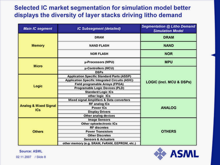
| Selected IC market segmentation for simulation model better displays the diversity of layer stacks driving litho demand Source: ASML Source: ASML |
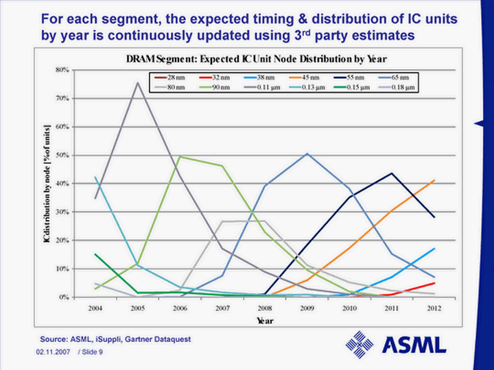
| For each segment, the expected timing & distribution of IC units by year is continuously updated using 3rd party estimates Source: ASML, iSuppli, Gartner Dataquest Source: ASML, iSuppli, Gartner Dataquest |
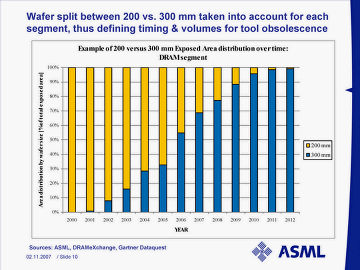
| Wafer split between 200 vs. 300 mm taken into account for each segment, thus defining timing & volumes for tool obsolescence Sources: ASML, DRAMeXchange, Gartner Dataquest Sources: ASML, DRAMeXchange, Gartner Dataquest |
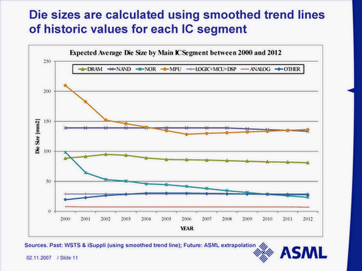
| Die sizes are calculated using smoothed trend lines of historic values for each IC segment Sources. Past: WSTS & iSuppli (using smoothed trend line); Future: ASML extrapolation Sources. Past: WSTS & iSuppli (using smoothed trend line); Future: ASML extrapolation |
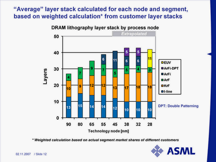
| "Average" layer stack calculated for each node and segment, based on weighted calculation* from customer layer stacks * Weighted calculation based on actual segment market shares of different customers * Weighted calculation based on actual segment market shares of different customers DRAM lithography layer stack by process node Extrapolated DPT: Double Patterning |
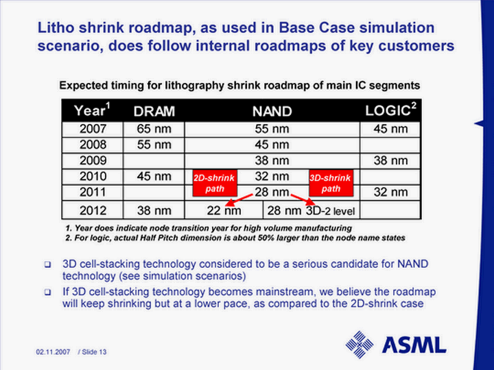
| Litho shrink roadmap, as used in Base Case simulation scenario, does follow internal roadmaps of key customers 3D cell-stacking technology considered to be a serious candidate for NAND technology (see simulation scenarios) If 3D cell-stacking technology becomes mainstream, we believe the roadmap will keep shrinking but at a lower pace, as compared to the 2D-shrink case 2D-shrink path 3D-shrink path 1. Year does indicate node transition year for high volume manufacturing 2. For logic, actual Half Pitch dimension is about 50% larger than the node name states Expected timing for lithography shrink roadmap of main IC segments |
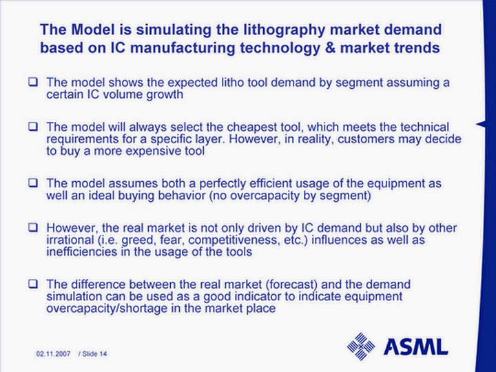
| The Model is simulating the lithography market demand based on IC manufacturing technology & market trends The model shows the expected litho tool demand by segment assuming a certain IC volume growth The model will always select the cheapest tool, which meets the technical requirements for a specific layer. However, in reality, customers may decide to buy a more expensive tool The model assumes both a perfectly efficient usage of the equipment as well an ideal buying behavior (no overcapacity by segment) However, the real market is not only driven by IC demand but also by other irrational (i.e. greed, fear, competitiveness, etc.) influences as well as inefficiencies in the usage of the tools The difference between the real market (forecast) and the demand simulation can be used as a good indicator to indicate equipment overcapacity/shortage in the market place |
| Contents Introduction Long-term market potential (2006 - 2012) ASML's Lithography Demand Simulation Model Some examples of simulated market scenarios Summary & Conclusions |
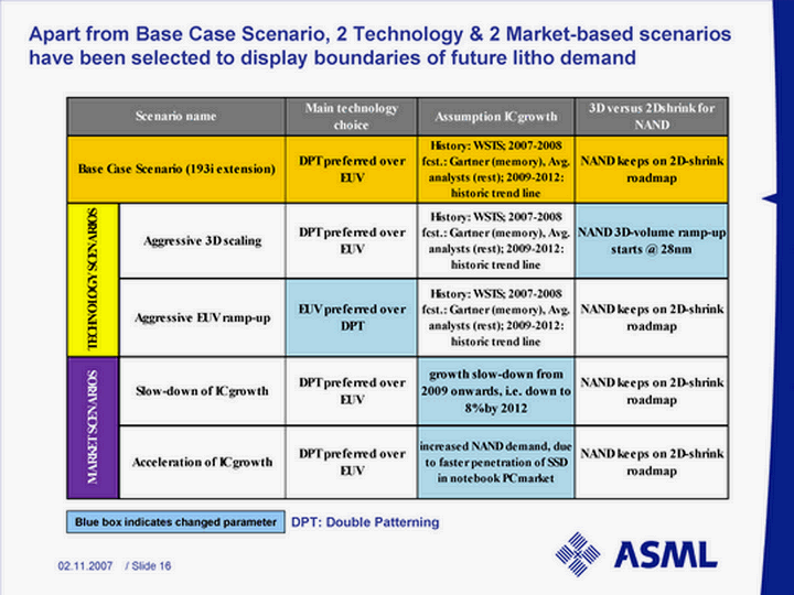
| Apart from Base Case Scenario, 2 Technology & 2 Market-based scenarios have been selected to display boundaries of future litho demand Blue box indicates changed parameter Blue box indicates changed parameter DPT: Double Patterning |
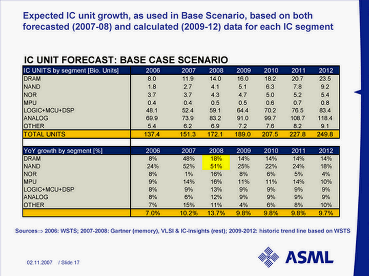
| Expected IC unit growth, as used in Base Scenario, based on both forecasted (2007-08) and calculated (2009-12) data for each IC segment Sources? 2006: WSTS; 2007-2008: Gartner (memory), VLSI & IC-Insights (rest); 2009-2012: historic trend line based on WSTS Sources? 2006: WSTS; 2007-2008: Gartner (memory), VLSI & IC-Insights (rest); 2009-2012: historic trend line based on WSTS |
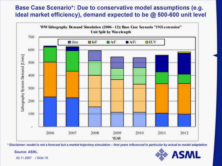
| Base Case Scenario*: Due to conservative model assumptions (e.g. ideal market efficiency), demand expected to be @ 500-600 unit level Source: ASML Source: ASML * Disclaimer: model is not a forecast but a market trajectory simulation - first years influenced in particular by actual to model adaptation |
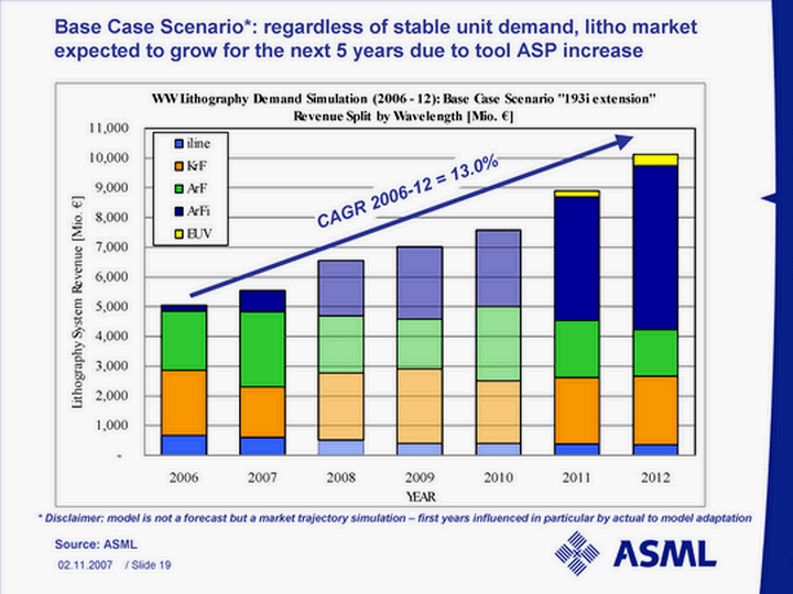
| Source: ASML Base Case Scenario*: regardless of stable unit demand, litho market expected to grow for the next 5 years due to tool ASP increase CAGR 2006-12 = 13.0% * Disclaimer: model is not a forecast but a market trajectory simulation - first years influenced in particular by actual to model adaptation |
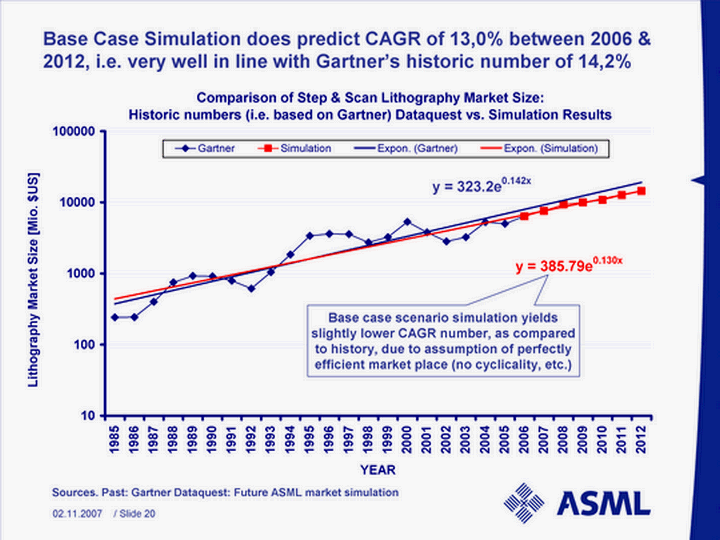
| Base Case Simulation does predict CAGR of 13,0% between 2006 & 2012, i.e. very well in line with Gartner's historic number of 14,2% Base case scenario simulation yields slightly lower CAGR number, as compared to history, due to assumption of perfectly efficient market place (no cyclicality, etc.) Sources. Past: Gartner Dataquest: Future ASML market simulation |
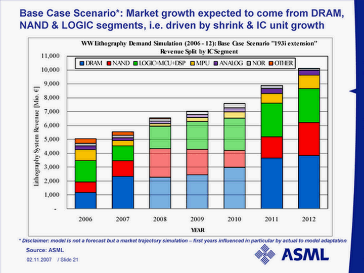
| Source: ASML Base Case Scenario*: Market growth expected to come from DRAM, NAND & LOGIC segments, i.e. driven by shrink & IC unit growth NAND & LOGIC segments, i.e. driven by shrink & IC unit growth NAND & LOGIC segments, i.e. driven by shrink & IC unit growth * Disclaimer: model is not a forecast but a market trajectory simulation - first years influenced in particular by actual to model adaptation |
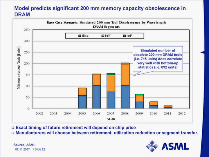
| Model predicts significant 200 mm memory capacity obsolescence in DRAM Source: ASML Source: ASML Simulated number of obsolete 200 mm DRAM tools (i.e. 715 units) does correlate very well with bottom-up statistics (i.e. 692 units) Exact timing of future retirement will depend on chip price Manufacturers will choose between retirement, utilization reduction or segment transfer |
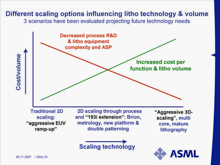
| Different scaling options influencing litho technology & volume 3 scenarios have been evaluated projecting future technology needs Decreased process R&D & litho equipment complexity and ASP Traditional 2D scaling: "aggressive EUV ramp-up" 2D scaling through process and "193i extension": Brion, metrology, new platform & double patterning "Aggressive 3D- scaling", multi core, mature lithography Increased cost per function & litho volume Scaling technology Cost/volume |
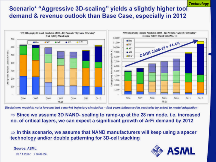
| Scenario* "Aggressive 3D-scaling" yields a slightly higher tool demand & revenue outlook than Base Case, especially in 2012 Since we assume 3D NAND- scaling to ramp-up at the 28 nm node, i.e. increased no. of critical layers, we can expect a significant growth of ArFi demand by 2012 ? In this scenario, we assume that NAND manufacturers will keep using a spacer technology and/or double patterning for 3D-cell stacking Technology Source: ASML CAGR 2006-12 = 14.4% CAGR 2006-12 = 14.4% Disclaimer: model is not a forecast but a market trajectory simulation - first years influenced in particular by actual to model adaptation |
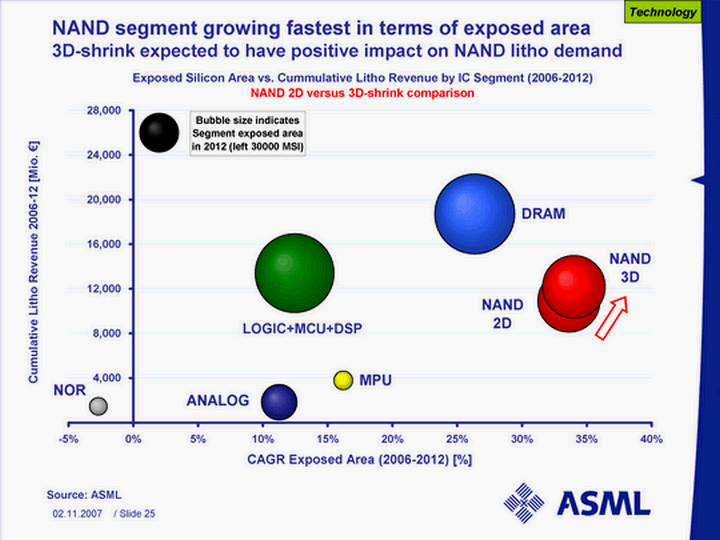
| NAND segment growing fastest in terms of exposed area 3D-shrink expected to have positive impact on NAND litho demand Technology Source: ASML |
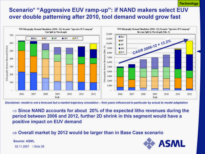
| Scenario* "Aggressive EUV ramp-up": if NAND makers select EUV over double patterning after 2010, tool demand would grow fast Since NAND accounts for about 20% of the expected litho revenues during the period between 2006 and 2012, further 2D shrink in this segment would have a positive impact on EUV demand ? Overall market by 2012 would be larger than in Base Case scenario Technology Source: ASML CAGR 2006-12 = 13.2% CAGR 2006-12 = 13.2% Disclaimer: model is not a forecast but a market trajectory simulation - first years influenced in particular by actual to model adaptation |
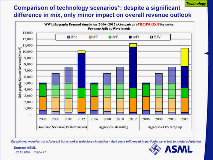
| Comparison of technology scenarios*: despite a significant difference in mix, only minor impact on overall revenue outlook Source: ASML Technology Technology Disclaimer: model is not a forecast but a market trajectory simulation - first years influenced in particular by actual to model adaptation |
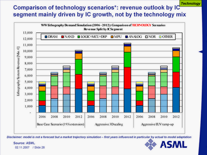
| Source: ASML Comparison of technology scenarios*: revenue outlook by IC segment mainly driven by IC growth, not by the technology mix Technology Technology Disclaimer: model is not a forecast but a market trajectory simulation - first years influenced in particular by actual to model adaptation |
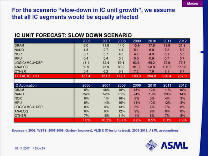
| For the scenario "slow-down in IC unit growth", we assume that all IC segments would be equally affected Sources? 2006: WSTS; 2007-2008: Gartner (memory), VLSI & IC-Insights (rest); 2009-2012: ASML assumptions Market Market |
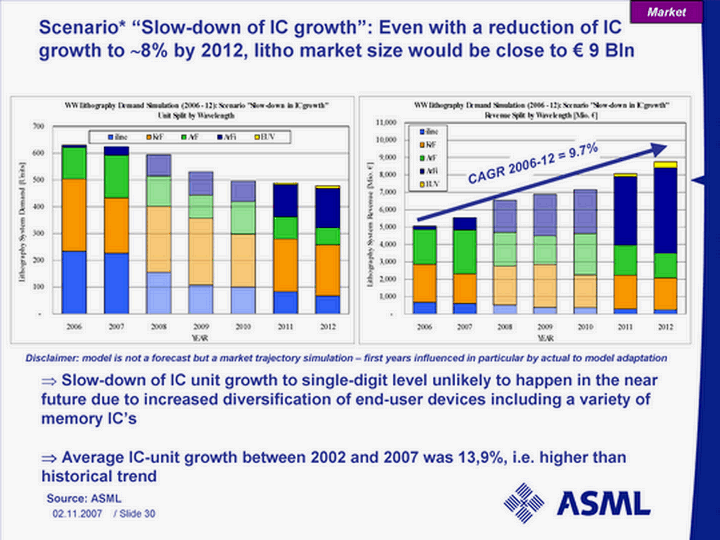
| Scenario* "Slow-down of IC growth": Even with a reduction of IC growth to ?8% by 2012, litho market size would be close to &128; 9 Bln Source: ASML Slow-down of IC unit growth to single-digit level unlikely to happen in the near future due to increased diversification of end-user devices including a variety of memory IC's ? Average IC-unit growth between 2002 and 2007 was 13,9%, i.e. higher than historical trend Market CAGR 2006-12 = 9.7% CAGR 2006-12 = 9.7% Disclaimer: model is not a forecast but a market trajectory simulation - first years influenced in particular by actual to model adaptation |
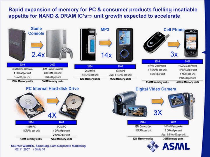
| Rapid expansion of memory for PC & consumer products fuelling insatiable appetite for NAND & DRAM IC's? unit growth expected to accelerate Source: WinHEC, Samsung, Lam Corporate Marketing 3x Cell Phone 4X PC Internal Hard-disk Drive 3X Digital Video Camera |
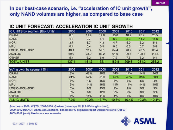
| In our best-case scenario, i.e. "acceleration of IC unit growth", only NAND volumes are higher, as compared to base case Sources? 2006: WSTS; 2007-2008: Gartner (memory), VLSI & IC-Insights (rest); 2009-2012 (NAND): ASML assumptions, based on PC segment report Deutsche Bank (Oct 07) 2009-2012 (rest): like base case scenario Market Market |
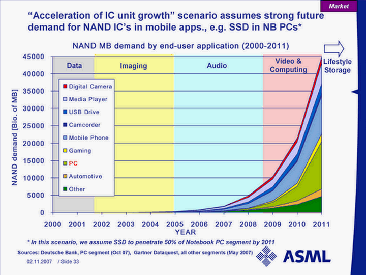
| 2000 2001 2002 2003 2004 2005 2006 2007 2008 2009 2010 2011 Other 0.41 0.75 1.74 3.55 5.81 20.75 91 263.9 625.84 1235.16 2348.98 4596.62 Automotive - 0.01 0.05 0.17 1.32 6.14 25.79 77.06 200.7 447.51 997.63 2119.37 PC - 0 0.02 0.24 0.62 2.9 10.59 28.91 299 1272 4144 13800 Gaming - - - - 0.33 9.03 30.17 87.03 166.09 427.87 944.73 2180.04 Mobile Phone 0.29 0.35 0.84 2.29 5.78 23.63 106.71 397.23 1208.09 2864.85 6322.95 10950.16 Camcorder 0.02 0.05 0.25 1.05 3.15 8.92 20.29 42.02 87.61 197.12 301.64 715.69 USB Drive 0.01 0.04 0.32 2.57 11.22 39.17 105.89 271.6 524.44 965.69 1772.37 2857.74 Media Player 0.06 0.17 0.44 1.02 9.61 54.81 200.05 432.68 1260.66 2153.26 3436.96 5795.65 Digital Camera 0.6 1.67 4.15 9.47 27.76 69.4 146.98 251.67 436.28 845.59 1211.08 1901.47 "Acceleration of IC unit growth" scenario assumes strong future demand for NAND IC's in mobile apps., e.g. SSD in NB PCs* Sources: Deutsche Bank, PC segment (Oct 07), Gartner Dataquest, all other segments (May 2007) Imaging Video & Computing Audio Data Lifestyle Storage Market * In this scenario, we assume SSD to penetrate 50% of Notebook PC segment by 2011 |
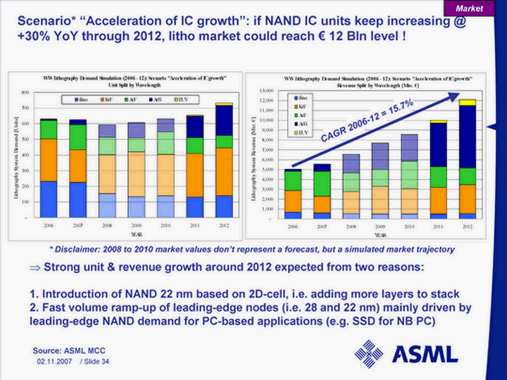
| Scenario* "Acceleration of IC growth": if NAND IC units keep increasing @ +30% YoY through 2012, litho market could reach &128; 12 Bln level ! Source: ASML MCC Strong unit & revenue growth around 2012 expected from two reasons: 1. Introduction of NAND 22 nm based on 2D-cell, i.e. adding more layers to stack 2. Fast volume ramp-up of leading-edge nodes (i.e. 28 and 22 nm) mainly driven by leading-edge NAND demand for PC-based applications (e.g. SSD for NB PC) Market CAGR 2006-12 = 15.7% * Disclaimer: 2008 to 2010 market values don't represent a forecast, but a simulated market trajectory * Disclaimer: 2008 to 2010 market values don't represent a forecast, but a simulated market trajectory |
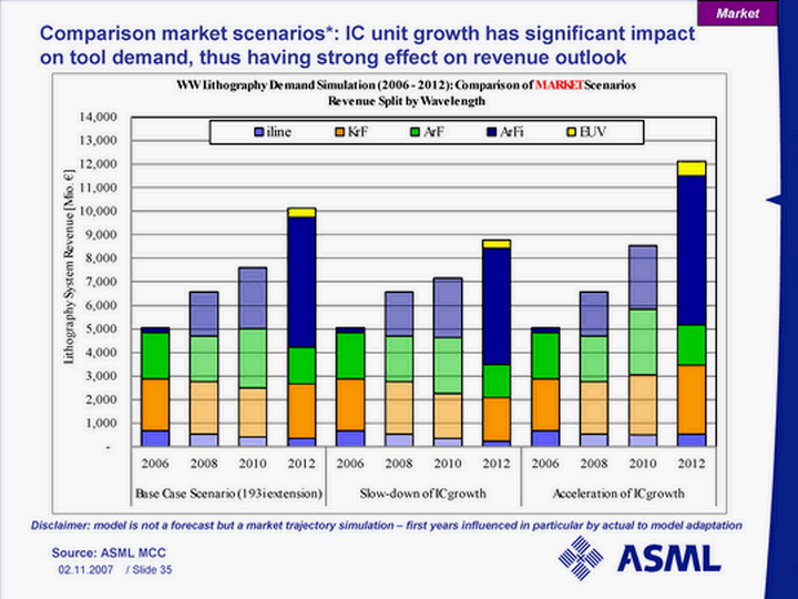
| Source: ASML MCC Comparison market scenarios*: IC unit growth has significant impact on tool demand, thus having strong effect on revenue outlook Market Disclaimer: model is not a forecast but a market trajectory simulation - first years influenced in particular by actual to model adaptation Disclaimer: model is not a forecast but a market trajectory simulation - first years influenced in particular by actual to model adaptation |
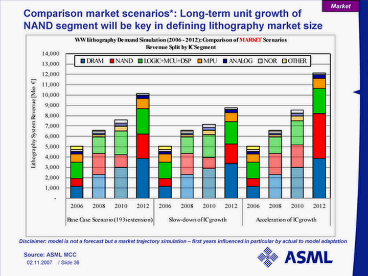
| Source: ASML MCC Comparison market scenarios*: Long-term unit growth of NAND segment will be key in defining lithography market size Market Disclaimer: model is not a forecast but a market trajectory simulation - first years influenced in particular by actual to model adaptation Disclaimer: model is not a forecast but a market trajectory simulation - first years influenced in particular by actual to model adaptation |
| Contents Introduction Long-term market potential (2006 - 2012) ASML's Lithography Demand Simulation Model Some examples of simulated market scenarios Summary & Conclusions |
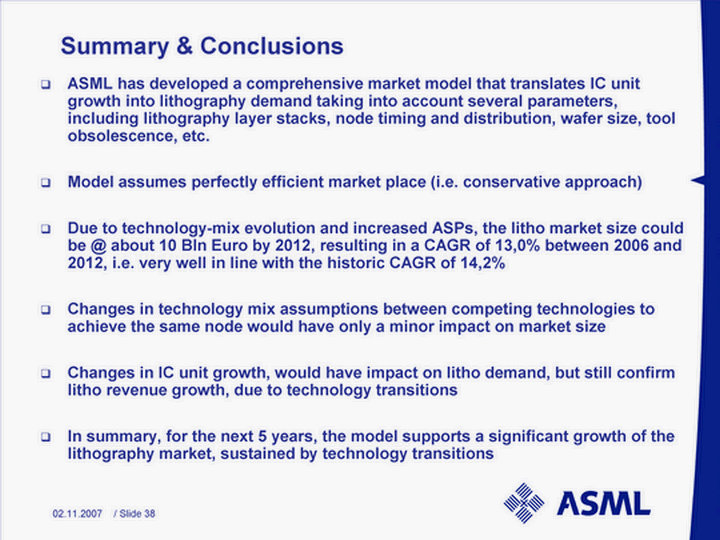
| Summary & Conclusions ASML has developed a comprehensive market model that translates IC unit growth into lithography demand taking into account several parameters, including lithography layer stacks, node timing and distribution, wafer size, tool obsolescence, etc. Model assumes perfectly efficient market place (i.e. conservative approach) Due to technology-mix evolution and increased ASPs, the litho market size could be @ about 10 Bln Euro by 2012, resulting in a CAGR of 13,0% between 2006 and 2012, i.e. very well in line with the historic CAGR of 14,2% Changes in technology mix assumptions between competing technologies to achieve the same node would have only a minor impact on market size Changes in IC unit growth, would have impact on litho demand, but still confirm litho revenue growth, due to technology transitions In summary, for the next 5 years, the model supports a significant growth of the lithography market, sustained by technology transitions |
| Commitment |