| Next Generation Lithography The road to cost-effective shrink Martin van den Brink Executive Vice President Marketing & Technology May 20, 2008 |
| Agenda Shrink roadmap Progress in immersion lithography A holistic approach to extend immersion lithography EUV the next production worthy shrink technology Economics of advanced lithography |
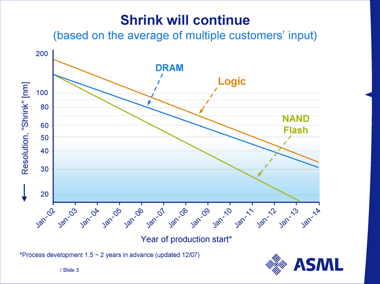
| Jan - 02 Jan - 03 Jan - 04 Jan - 05 Jan - 06 Jan - 07 Jan - 08 Jan - 09 Jan - 10 Jan - 11 Jan - 12 Jan - 13 Jan - 14 Year of production start* Resolution, "Shrink" [nm] 100 80 60 40 Logic NAND Flash DRAM 30 20 50 *Process development 1.5 ~ 2 years in advance (updated 12/07) 200 Shrink will continue (based on the average of multiple customers' input) |
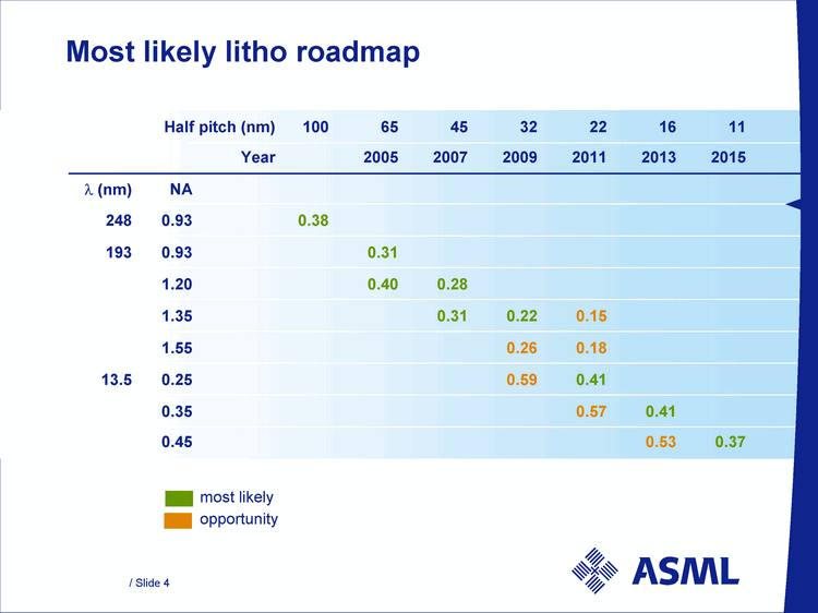
| Most likely litho roadmap Half pitch (nm) Half pitch (nm) Half pitch (nm) Half pitch (nm) Half pitch (nm) 100 65 45 32 22 16 11 Year Year Year 2005 2007 2009 2011 2013 2015 ? (nm) NA NA 248 0.93 0.93 0.38 0.38 193 0.93 0.93 0.31 1.20 1.20 0.40 0.28 1.35 1.35 0.31 0.22 0.15 1.55 1.55 0.26 0.18 13.5 0.25 0.25 0.59 0.41 0.35 0.35 0.57 0.41 0.45 0.45 0.53 0.37 most likely opportunity |
| Agenda Shrink roadmap Progress in immersion lithography A holistic approach to extend immersion lithography EUV the next production worthy shrink technology Economics of advanced lithography |
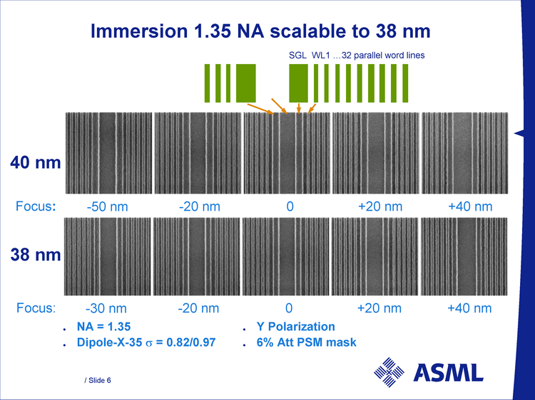
| Immersion 1.35 NA scalable to 38 nm SGL WL1 ...32 parallel word lines Focus: 40 nm 38 nm - -20 nm 0 +20 nm +40 nm - -50 nm - -20 nm 0 +20 nm +40 nm - -30 nm Focus: NA = 1.35 Dipole-X-35 ? = 0.82/0.97 Y Polarization 6% Att PSM mask |
| Shrink roadmap Progress in immersion lithography A holistic approach to extend immersion lithography Double patterning Optimize performance using computational lithography Reduce variability using intra-field litho correction EUV the next production worthy shrink technology Economics of advanced lithography Agenda |
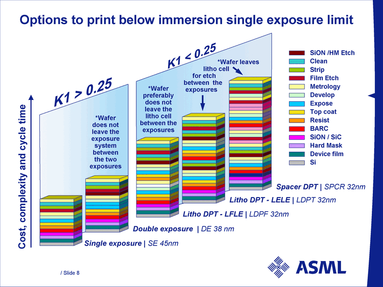
| Spacer DPT | SPCR 32nm Litho DPT - LELE | LDPT 32nm Litho DPT - LFLE | LDPF 32nm Double exposure | DE 38 nm SiON /HM Etch Clean Strip Film Etch Metrology Develop Expose Top coat Resist BARC SiON / SiC Hard Mask Device film Si Single exposure | SE 45nm Options to print below immersion single exposure limit Cost, complexity and cycle time *Wafer does not leave the exposure system between the two exposures *Wafer preferably does not leave the litho cell between the exposures *Wafer leaves litho cell for etch between the exposures |
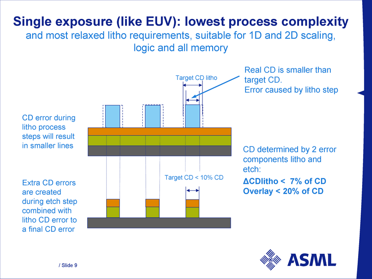
| Single exposure (like EUV): lowest process complexity and most relaxed litho requirements, suitable for 1D and 2D scaling, logic and all memory Real CD is smaller than target CD. Error caused by litho step CD error during litho process steps will result in smaller lines Extra CD errors are created during etch step combined with litho CD error to a final CD error Target CD litho Target CD < 10% CD CD determined by 2 error components litho and etch: ^CDlitho < 7% of CD Overlay < 20% of CD |
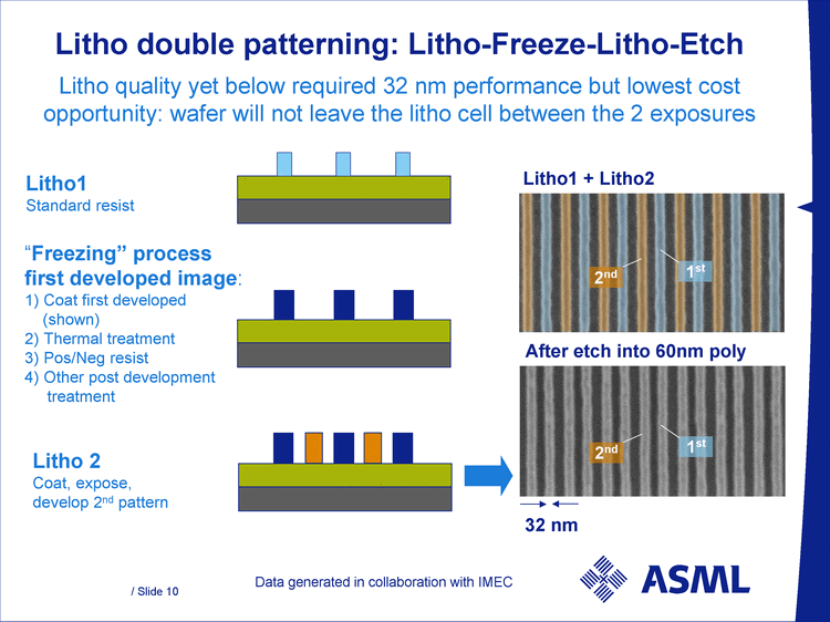
| Litho1 Standard resist "Freezing" process first developed image: Coat first developed (shown) Thermal treatment Pos/Neg resist Other post development treatment Litho 2 Coat, expose, develop 2nd pattern Litho double patterning: Litho-Freeze-Litho-Etch Litho quality yet below required 32 nm performance but lowest cost opportunity: wafer will not leave the litho cell between the 2 exposures 32 nm Litho1 + Litho2 After etch into 60nm poly 2nd 1st 2nd 1st Data generated in collaboration with IMEC |
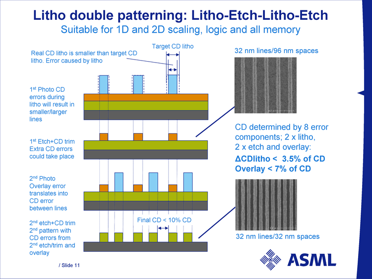
| Litho double patterning: Litho-Etch-Litho-Etch Suitable for 1D and 2D scaling, logic and all memory 1st Photo CD errors during litho will result in smaller/larger lines 1st Etch+CD trim Extra CD errors could take place 2nd Photo Overlay error translates into CD error between lines 2nd etch+CD trim 2nd pattern with CD errors from 2nd etch/trim and overlay 32 nm lines/96 nm spaces 32 nm lines/32 nm spaces Real CD litho is smaller than target CD litho. Error caused by litho Target CD litho Final CD < 10% CD CD determined by 8 error components; 2 x litho, 2 x etch and overlay: ^CDlitho < 3.5% of CD Overlay < 7% of CD |
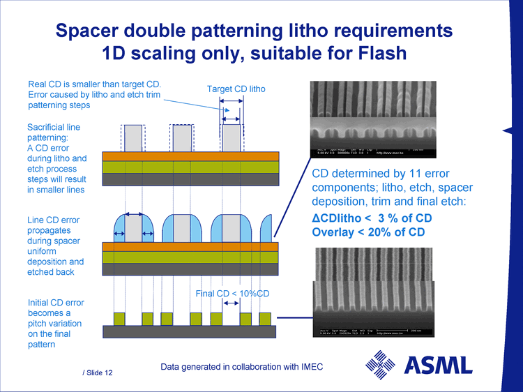
| CD determined by 11 error components; litho, etch, spacer deposition, trim and final etch: ^CDlitho < 3 % of CD Overlay < 20% of CD Spacer double patterning litho requirements 1D scaling only, suitable for Flash Real CD is smaller than target CD. Error caused by litho and etch trim patterning steps Sacrificial line patterning: A CD error during litho and etch process steps will result in smaller lines Target CD litho Final CD < 10%CD Line CD error propagates during spacer uniform deposition and etched back Initial CD error becomes a pitch variation on the final pattern Data generated in collaboration with IMEC |
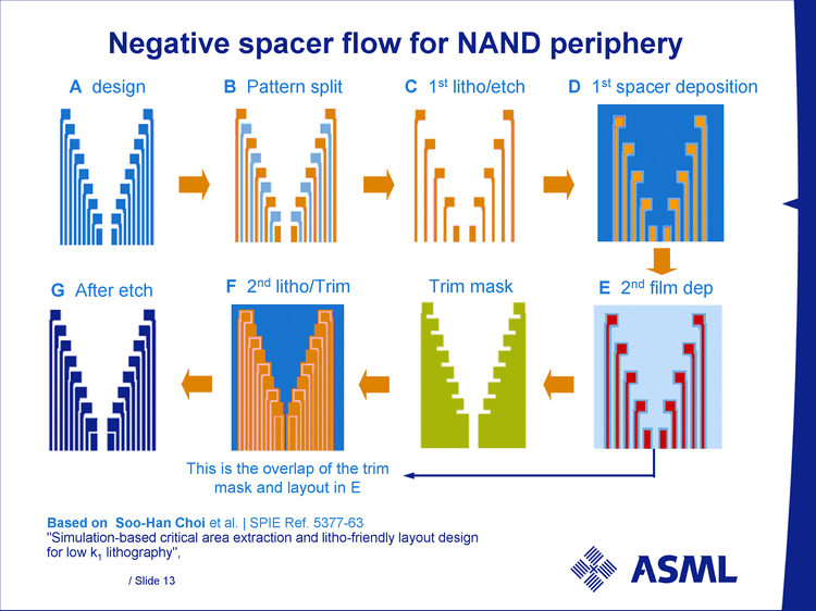
| Negative spacer flow for NAND periphery G After etch Trim mask B Pattern split C 1st litho/etch D 1st spacer deposition A design Based on Soo-Han Choi et al. | SPIE Ref. 5377-63 "Simulation-based critical area extraction and litho-friendly layout design for low k1 lithography", F 2nd litho/Trim This is the overlap of the trim mask and layout in E E 2nd film dep |
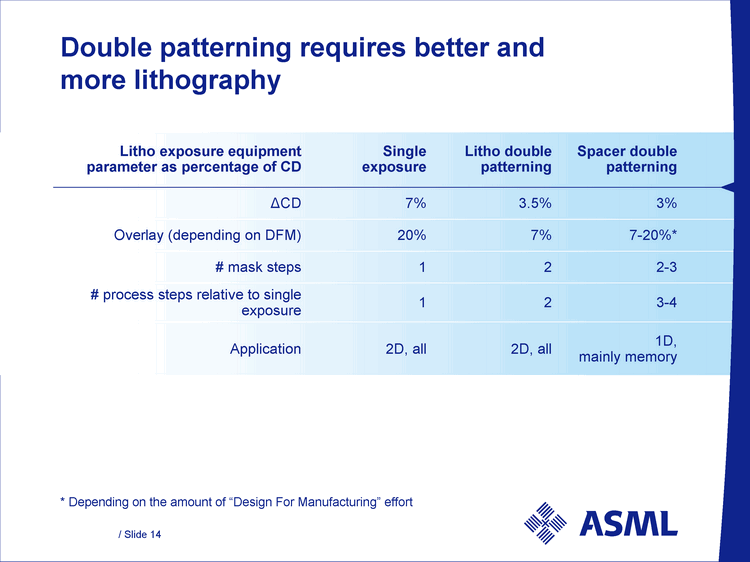
| Double patterning requires better and more lithography Litho exposure equipment parameter as percentage of CD Single exposure Litho double patterning Spacer double patterning ^CD 7% 3.5% 3% Overlay (depending on DFM) 20% 7% 7-20%* # mask steps 1 2 2-3 # process steps relative to single exposure 1 2 3-4 Application 2D, all 2D, all 1D, mainly memory * Depending on the amount of "Design For Manufacturing" effort |
| Shrink roadmap Progress in immersion lithography A holistic approach to extend immersion lithography Double patterning Optimize performance using computational lithography Reduce variability using intra-field litho correction EUV the next production worthy shrink technology Economics of advanced lithography Agenda |
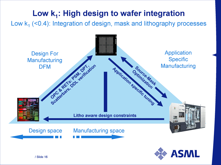
| Design For Manufacturing DFM Application Specific Manufacturing Design space Manufacturing space Litho aware design constraints OPC & RETs: PSM, DPT, Scatterbars, DDL verification Application specific tuning Source-Mask Optimization Low k1: High design to wafer integration Low k1 (<0.4): Integration of design, mask and lithography processes |
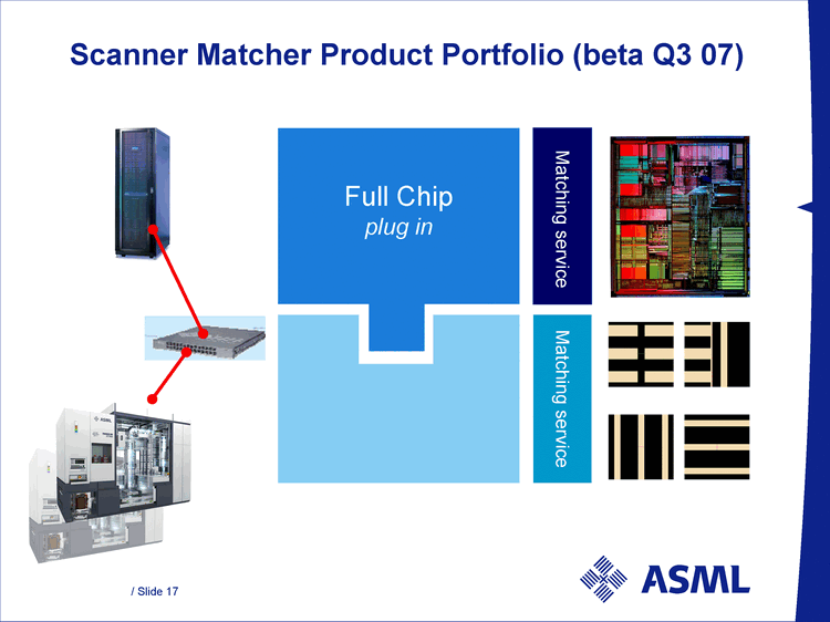
| Scanner Matcher Product Portfolio (beta Q3 07) Full Chip plug in Matching service Matching service |
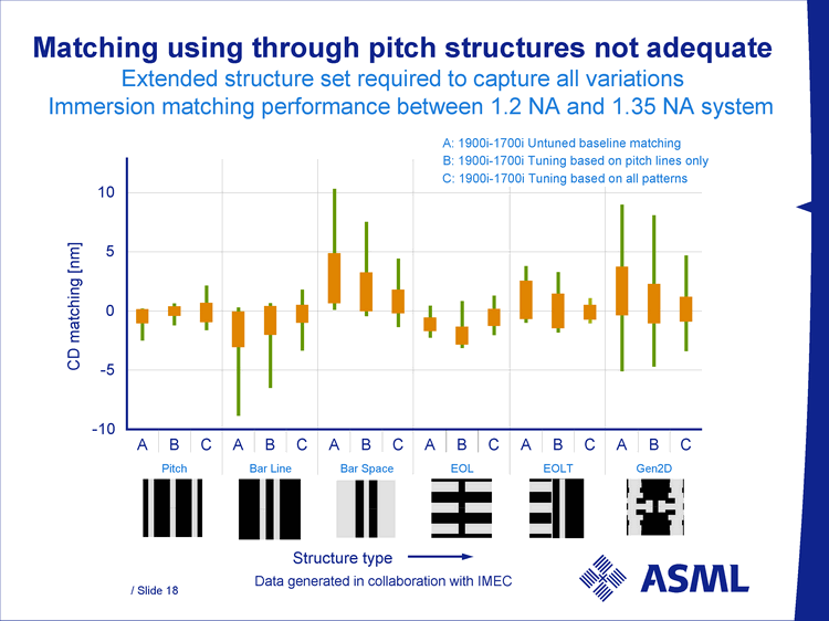
| Matching using through pitch structures not adequate Extended structure set required to capture all variations Structure type Structure type CD matching [nm] Immersion matching performance between 1.2 NA and 1.35 NA system - -10 - -5 0 5 10 A B C A B C A B C A B C A B C A B C Pitch Bar Line Bar Space EOL EOLT Gen2D A: 1900i-1700i Untuned baseline matching B: 1900i-1700i Tuning based on pitch lines only C: 1900i-1700i Tuning based on all patterns Data generated in collaboration with IMEC |
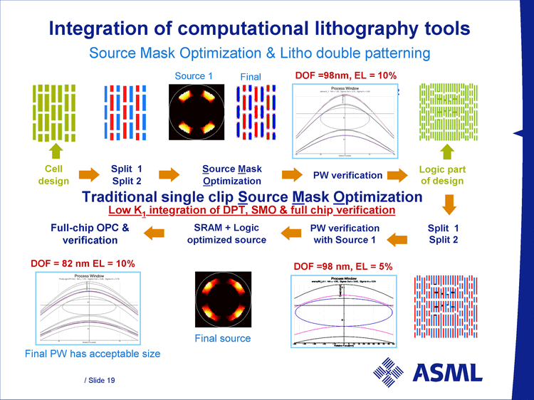
| Integration of computational lithography tools Source Mask Optimization & Litho double patterning Low K1 integration of DPT, SMO & full chip verification Traditional single clip Source Mask Optimization Split 1 Split 2 Source Mask Optimization Cell design PW verification Split 1 Split 2 Final Source 1 DOF =98nm, EL = 10% Logic part of design SRAM + Logic optimized source Split 1 Split 2 Full-chip OPC & verification verification verification DOF = 82 nm EL = 10% Final source PW verification with Source 1 DOF =98 nm, EL = 5% Final PW has acceptable size |
| Shrink roadmap Progress in immersion lithography A holistic approach to extend immersion lithography Double patterning Optimize performance using computational lithography Reduce variability using intra-field litho correction EUV the next production worthy shrink technology Economics of advanced lithography Agenda |
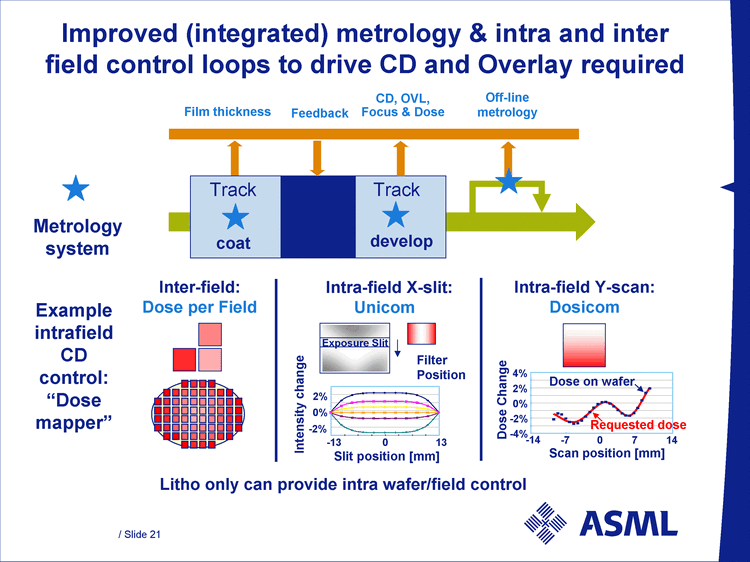
| Improved (integrated) metrology & intra and inter field control loops to drive CD and Overlay required develop Track Off-line metrology CD, OVL, Focus & Dose Film thickness Feedback Example intrafield CD control: "Dose mapper" Inter-field: Dose per Field Intra-field Y-scan: Dosicom - -2% 0% 2% 4% - -4% - -14 - -7 0 7 14 Dose Change Dose on wafer Requested dose Scan position [mm] Intra-field X-slit: Unicom - -2% 0% 2% - -13 0 13 Slit position [mm] Intensity change Filter Position Exposure Slit Litho only can provide intra wafer/field control coat Track Metrology system |
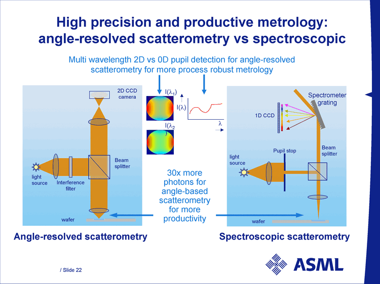
| High precision and productive metrology: angle-resolved scatterometry vs spectroscopic Multi wavelength 2D vs 0D pupil detection for angle-resolved scatterometry for more process robust metrology ? I(?) 30x more photons for angle-based scatterometry for more productivity Spectrometer grating Beam splitter 1D CCD light source wafer Pupil stop light source wafer Interference filter 2D CCD camera Beam splitter Angle-resolved scatterometry Spectroscopic scatterometry I(?1) I(?2 ) |
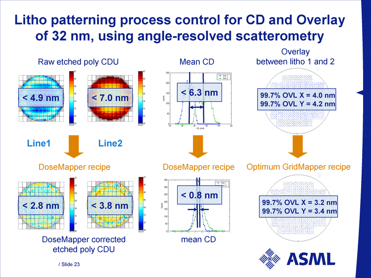
| Litho patterning process control for CD and Overlay of 32 nm, using angle-resolved scatterometry Overlay between litho 1 and 2 DoseMapper recipe Line1 Line2 Raw etched poly CDU DoseMapper recipe Optimum GridMapper recipe DoseMapper corrected etched poly CDU Mean CD mean CD < 4.9 nm < 7.0 nm < 3.8 nm < 2.8 nm 99.7% OVL X = 3.2 nm 99.7% OVL Y = 3.4 nm < 0.8 nm < 6.3 nm 99.7% OVL X = 4.0 nm 99.7% OVL Y = 4.2 nm |
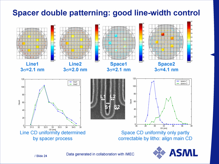
| Spacer double patterning: good line-width control L1 L2 S1 S2 Line1 3s=2.1 nm Line CD uniformity determined by spacer process Space CD uniformity only partly correctable by litho: align main CD Line2 3s=2.0 nm Space1 3s=2.1 nm Space2 3s=4.1 nm Data generated in collaboration with IMEC |
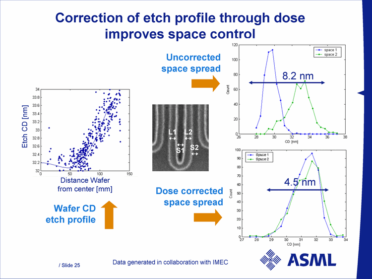
| Correction of etch profile through dose improves space control Distance Wafer from center [mm] L1 L2 S1 S2 8.2 nm 4.5 nm Etch CD [nm] Wafer CD etch profile Uncorrected space spread Dose corrected space spread Data generated in collaboration with IMEC |
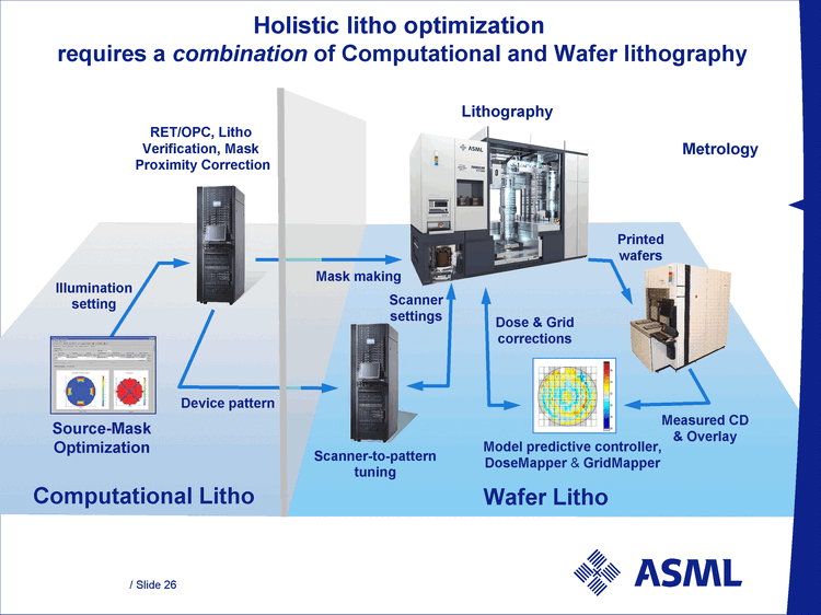
| Lithography Holistic litho optimization requires a combination of Computational and Wafer lithography Source-Mask Optimization RET/OPC, Litho Verification, Mask Proximity Correction Scanner-to-pattern tuning Metrology Model predictive controller, DoseMapper & GridMapper Illumination setting Device pattern Printed wafers Measured CD & Overlay Computational Litho Wafer Litho Mask making Dose & Grid corrections Scanner settings |
| Shrink roadmap Progress in immersion lithography A holistic approach to extend immersion lithography EUV the next production worthy shrink technology Economics of advanced lithography Agenda |
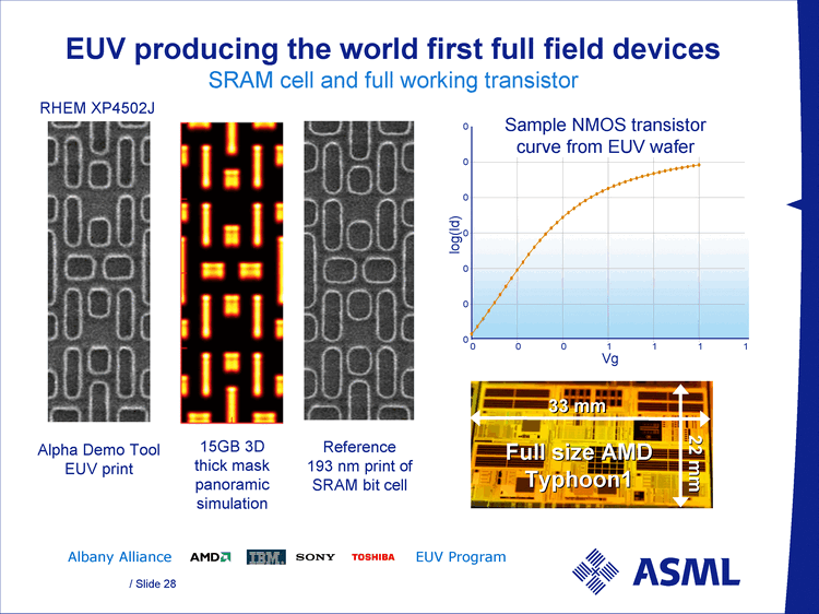
| EUV producing the world first full field devices SRAM cell and full working transistor Alpha Demo Tool EUV print 15GB 3D thick mask panoramic simulation Reference 193 nm print of SRAM bit cell Sample NMOS transistor curve from EUV wafer 0 0 0 0 0 0 0 0 0 0 1 1 1 1 Vg log(Id) Albany Alliance EUV Program RHEM XP4502J Full size AMD Typhoon1 33 mm 22 mm Full size AMD Typhoon1 33 mm 22 mm |
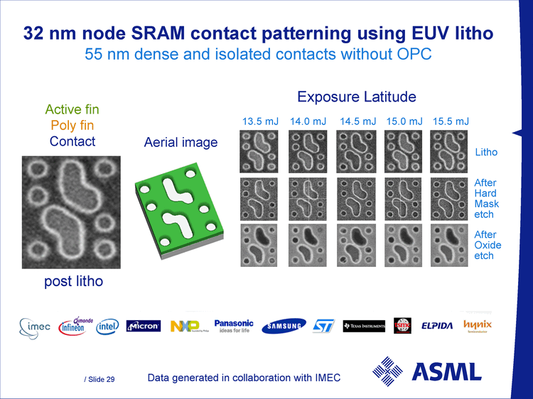
| After Hard Mask etch 13.5 mJ 14.0 mJ 14.5 mJ 15.0 mJ 15.5 mJ Litho After Oxide etch Exposure Latitude Data generated in collaboration with IMEC Aerial image 32 nm node SRAM contact patterning using EUV litho 55 nm dense and isolated contacts without OPC Active fin Poly fin Contact post litho |
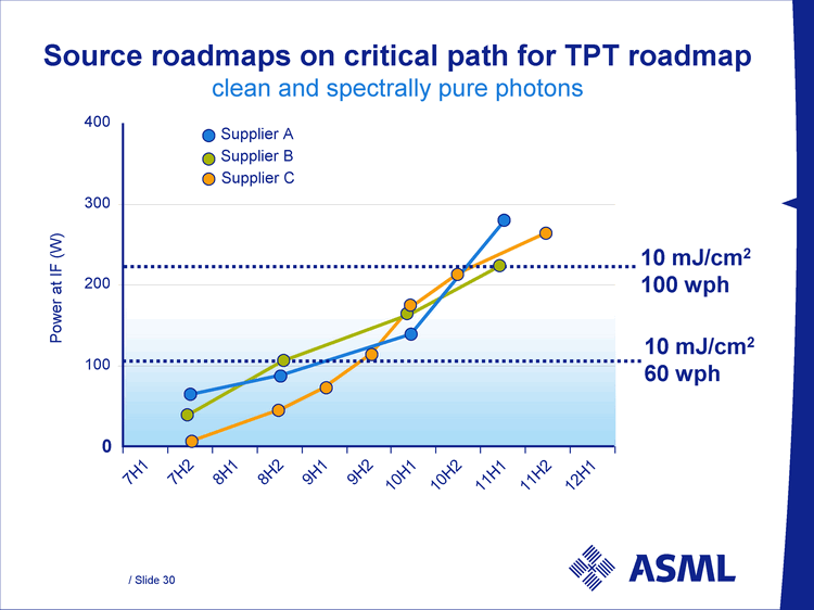
| 0 100 200 300 400 7H1 7H2 8H1 8H2 9H1 9H2 10H1 10H2 11H1 11H2 12H1 Power at IF (W) Supplier A Supplier B Supplier C Source roadmaps on critical path for TPT roadmap clean and spectrally pure photons 10 mJ/cm2 60 wph 10 mJ/cm2 100 wph |
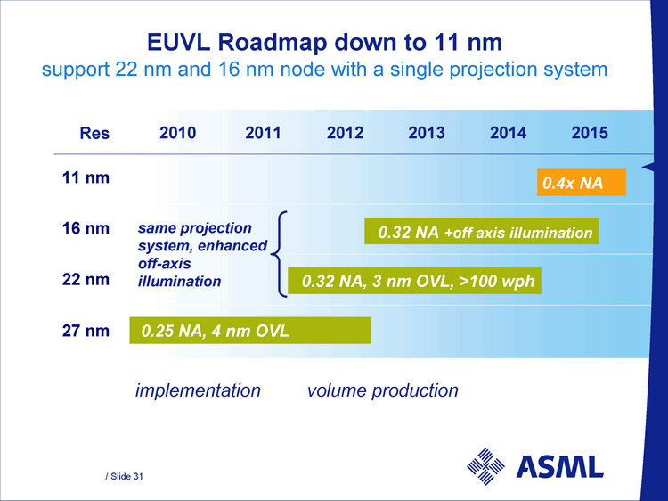
| EUVL Roadmap down to 11 nm support 22 nm and 16 nm node with a single projection system same projection system, enhanced off-axis illumination implementation volume production Res 11 nm 16 nm 22 nm 27 nm 2014 2015 2013 2010 2011 2012 0.32 NA, 3 nm OVL, >100 wph 0.25 NA, 4 nm OVL 0.4x NA 0.32 NA +off axis illumination |
| Shrink roadmap Progress in immersion lithography A holistic approach to extend immersion lithography EUV the next production worthy shrink technology Economics of advanced lithography Agenda |
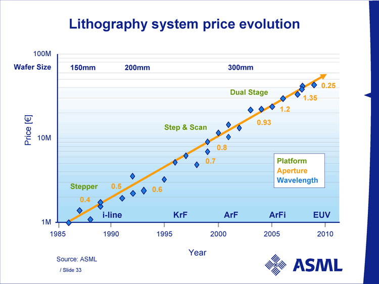
| Lithography system price evolution 1M 10M 100M 1985 1990 1995 2000 2005 2010 Year Price [€] i-line 300mm 200mm 150mm KrF ArF ArFi EUV Wafer Size Stepper Platform Aperture Wavelength Step & Scan Dual Stage 0.4 0.5 0.6 0.7 0.8 0.93 1.2 0.25 Source: ASML 1.35 |
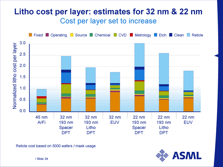
| Litho cost per layer: estimates for 32 nm & 22 nm Cost per layer set to increase Reticle cost based on 5000 wafers / mask usage Fixed Operating Source Chemical CVD Metrology Etch Clean Reticle 0.0 0.5 1.0 1.5 2.0 2.5 3.0 32 nm 193 nm Spacer DPT Normalized litho cost per layer 45 nm ArFi 32 nm 193 nm Litho DPT 22 nm 193 nm Spacer DPT 32 nm EUV 22 nm 193 nm Litho DPT 22 nm EUV |
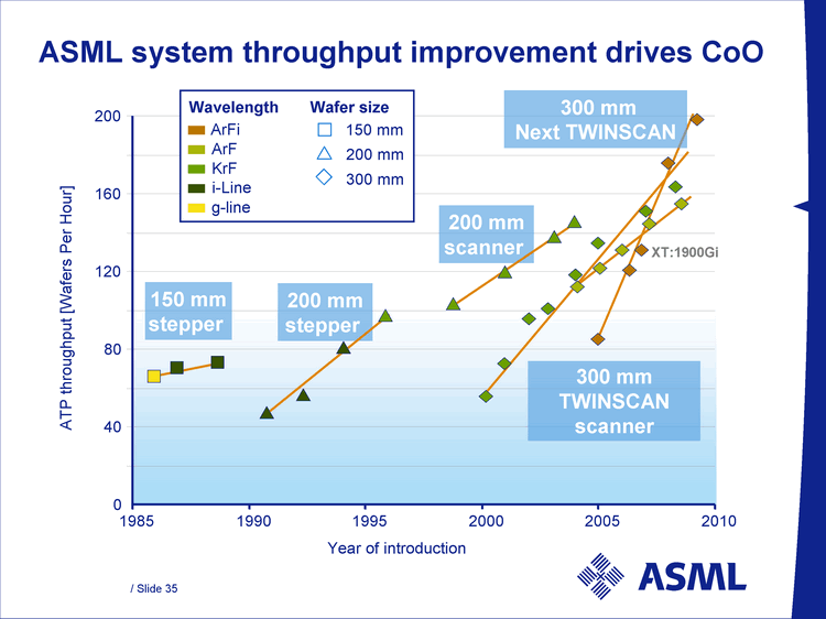
| ASML system throughput improvement drives CoO 0 40 80 120 160 200 1985 1990 1995 2000 2005 2010 g-line i-Line KrF ArF ArFi Wavelength Wafer size Year of introduction ATP throughput [Wafers Per Hour] 200 mm stepper 150 mm stepper 200 mm scanner 300 mm TWINSCAN scanner XT:1900Gi 300 mm Next TWINSCAN 150 mm 200 mm 300 mm |
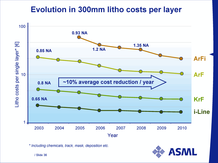
| Evolution in 300mm litho costs per layer * Including chemicals, track, mask, deposition etc. Litho costs per single layer* [€] 2003 2004 2005 2006 2007 2008 2009 2010 Year 1 10 100 ~10% average cost reduction / year 0.93 NA 1.35 NA 1.2 NA ArFi ArF KrF i-Line 0.85 NA 0.8 NA 0.65 NA |
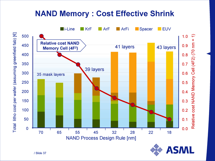
| NAND Memory : Cost Effective Shrink 0 50 100 150 200 250 300 350 400 450 500 70 65 55 45 32 28 22 18 0.0 0.1 0.2 0.3 0.4 0.5 0.6 0.7 0.8 0.9 1.0 i-Line KrF ArF ArFi Spacer EUV NAND Process Design Rule [nm] Total litho cost per wafer (assuming greenfield fab) [€] 35 mask layers 39 layers 41 layers 43 layers Relative cost NAND Memory Cell (4F2) Relative cost NAND Memory Cell (4F2) (70 nm = 1) |
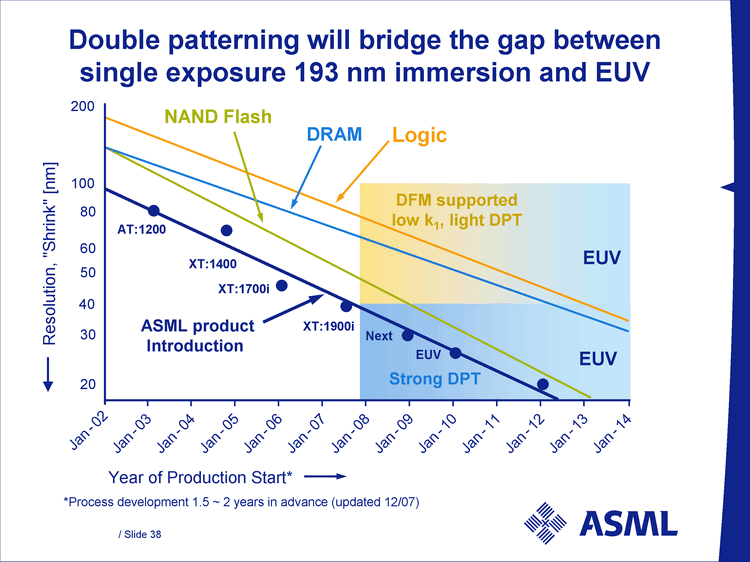
| Strong DPT EUV DFM supported low k1, light DPT EUV Year of Production Start* Resolution, "Shrink" [nm] 100 80 60 Logic NAND Flash DRAM 30 20 50 *Process development 1.5 ~ 2 years in advance (updated 12/07) 200 Double patterning will bridge the gap between single exposure 193 nm immersion and EUV AT:1200 XT:1400 XT:1900i Next EUV ASML product Introduction 40 XT:1700i Jan - 02 Jan - 03 Jan - 04 Jan - 05 Jan - 06 Jan - 07 Jan - 08 Jan - 09 Jan - 10 Jan - 11 Jan - 12 Jan - 13 Jan - 14 |

| Commitment |