40 nm and below
Extending water-based immersion towards the limit
Martin van den Brink
Executive Vice President Marketing and Technology

Contents
Inspiration: Market drivers
Immersion: Ramping to volume production
Innovation: Pushing ArF Lithography to 40 nm and below
/ Slide 2
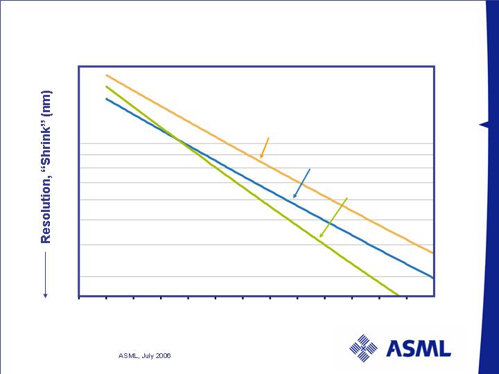
Customers’ appetite for shrink continues unabated
10
12
200
100
80
60
40
Logic
DRAM
NAND
11
07
09
08
04
06
05
01
03
02
00
/ Slide 3
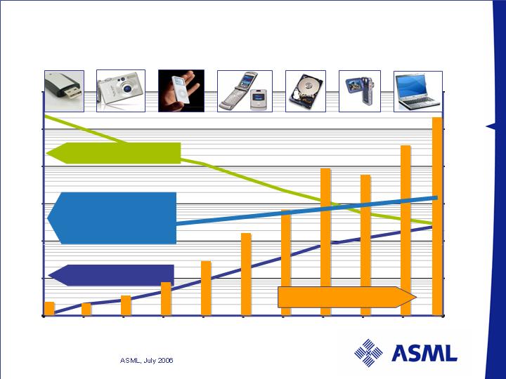
Shrink drives cost per function and market growth
Source: Gartner Dataquest, iSuppli, ASML
2000
2001
2002
2003
2004
2005
2006
2007
2008
2009
2010
NAND cost, $ / GB
NAND size, GB
0.01
0.10
1.00
10.0
100
1,000
10,000
0
5,000
10,000
15,000
20,000
25,000
30,000
NAND Revenue, M$
Projected cross-
over
HDD - NAND, GB
60-80 GB
2-16 GB
80-150 GB
1 GB
4 GB
8 GB
10-20 GB
/ Slide 4
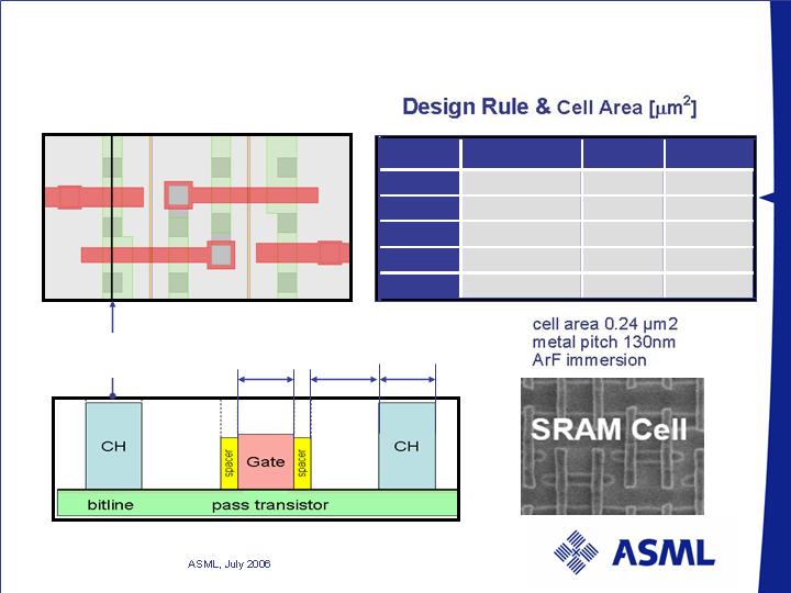
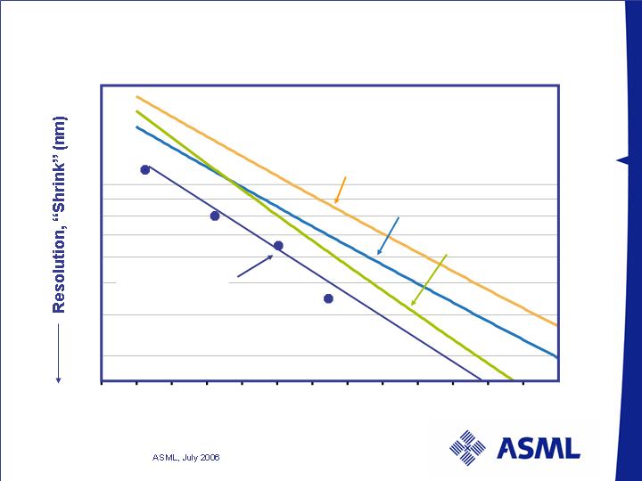
Resolution, CD uniformity & overlay drive shrink
Layout 6 transistor SRAM Cell
CD
CD
CDU &
Overlay
X-section
through Cell
Source: IMEC, TI
Node
Aggressive
Typical
Relaxed
130 nm
2.00
2.50
3.00
90 nm
1.00
1.25
1.50
65 nm
0.45
0.55
0.80
45 nm
0.20
0.27
0.34
32 nm
0.10
0.13
0.19
/ Slide 5
Source: IMEC
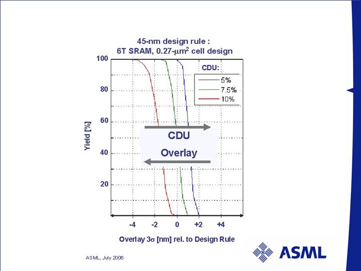
CD control and overlay are critical for device yield
/ Slide 6
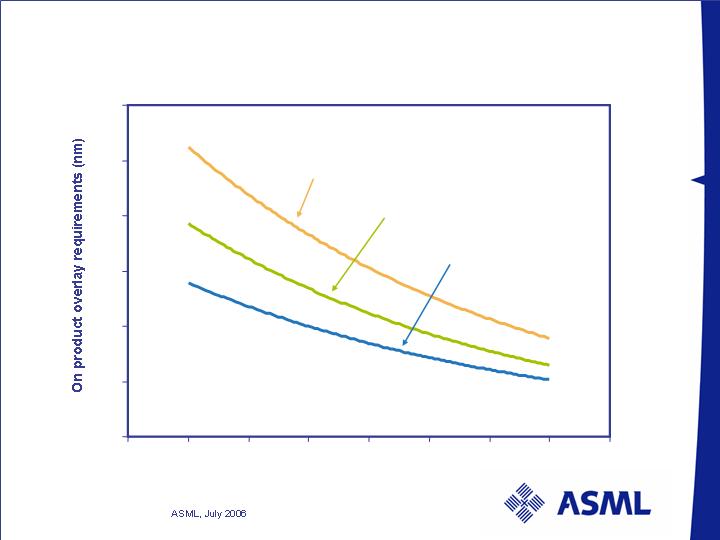
Shrink drives overlay requirements
0
5
10
15
20
25
30
2004
2005
2006
2007
2008
2009
2010
2011
2012
NAND
DRAM
Logic
/ Slide 7

Lithography drives increased die per wafer
Typical
Aggressive
Relaxed
868
1234
1803
2344
28 mm2
37 mm2
54 mm2
76 mm2
Die Size
Die / Wafer
45 nm
32 nm
Design Rule:
45 nm
32 nm
Resolution (CD)
256 MB SRAM example
/ Slide 8
0.00
0.50
1.00
1.50
2.00
2.50
3.00
3.50
65
45
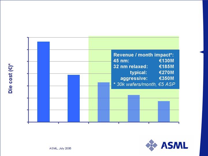
Increased die per wafer drives lower cost die
* Assuming 20% wafer processing cost
increase per node, 65nm = €1200 / wafer,
die yield = 85%
Design Rule [nm]
Relaxed
Typical
Aggressive
256 MB SRAM
32-nm node
/ Slide 9
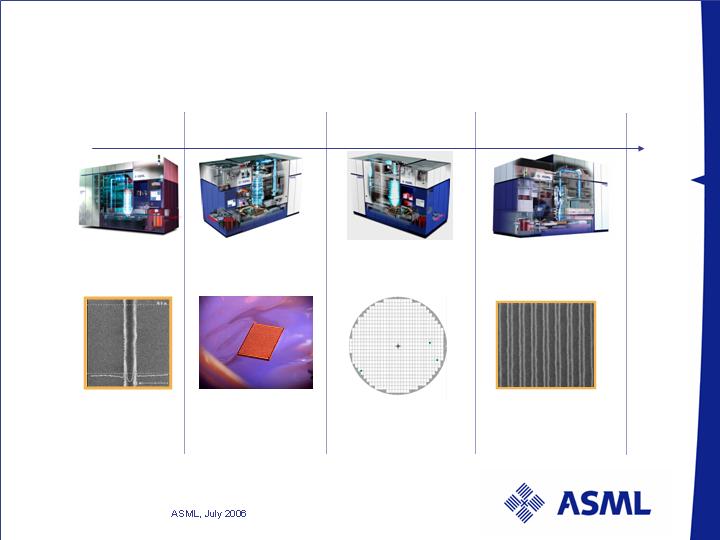
ASML products are key enablers for shrink
10
12
200
100
80
60
40
Logic
DRAM
NAND
11
07
09
08
04
06
05
01
03
02
00
ASML Product
Introduction
XT:1400
XT:1700i
AT:1200
AT:850
/ Slide 10
Performance
Size (=Cost)
Yield
Cost
Size (=cost)
Yield
Lithography
Productivity
Overlay
Resolution
CD Control
Lithography: drives Performance, Cost, Size, Yield
A key enabler for the semiconductor industry
Lithography
/ Slide 11

Contents
Inspiration: Market drivers
Immersion: Ramping to volume production
Innovation: Pushing ArF Lithography to 40 nm and below
/ Slide 12
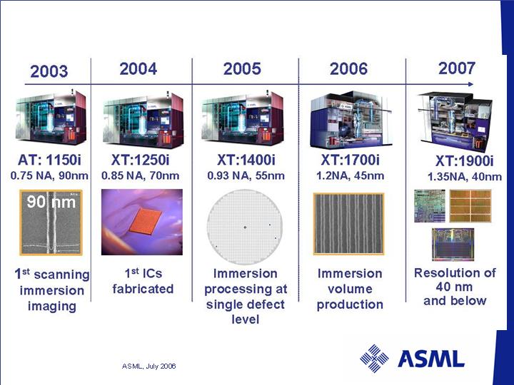
ASML achievements in immersion leadership
2003
90 nm
1st scanning
immersion
imaging
XT:1250i
0.85 NA, 70 nm
2004
AT:1150i
0.75 NA, 90 nm
1st ICs
fabricated
2005
XT:1400i
0.93 NA, 65 nm
42 nm
Immersion
Volume
Production
2006
XT:1700i
1.2NA, 45 nm
Immersion
processing at
single defect
level
/ Slide 13
THIS QUARTER 2006:
SHIPPING 500th TWINSCAN SYSTEM
TWINSCAN, with dual wafer stages, is the economically
and technically proven lithography solution
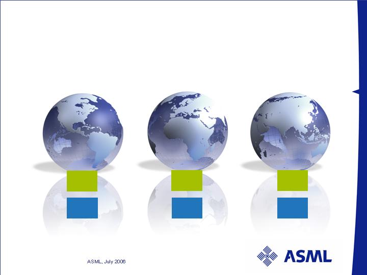
8
US
Europe
Asia
125
Total & Immersion
2
10
35
340
/ Slide 14
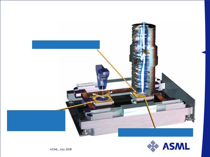
TWINSCAN dual stages are ideal for immersion
Immersion exposure
Immersion shower head
Dry alignment
Dry wafer mapping
(focus & levelling)
/ Slide 15
TWINSCAN dual wafer stages offer the most extensive
integrated metrology and calibration capability
Wafer height map
Calibration of process -
focus
Alignment mark positions
Pupil intensity and polarization
Slit uniformity
Lens aberrations
Reticle shape deformations
Expose position
Metrology position
Dual wafer stage concept is key enabler for automatic integrated
MEASUREMENT - CALIBRATION - OPTIMIZATION
Both wafer
stages are being
used in both
positions
Both wafer stages
contain integrated
metrology sensors
/ Slide 16
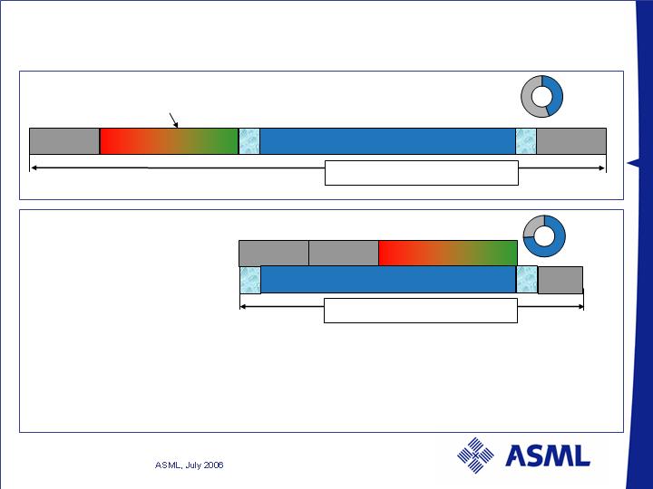
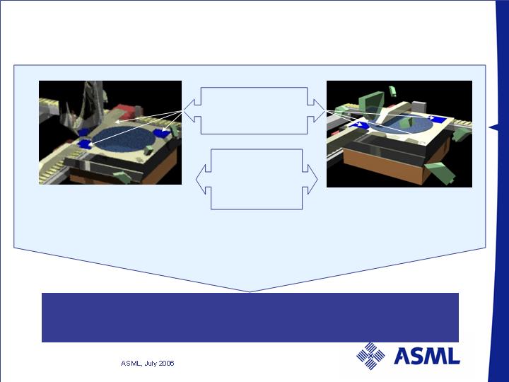
Dual wafer stages
Dual wafer stages enable parallel wafer
processing for unparalleled throughput
SWAP
UNLOAD
LOAD
Metrology position
Expose position
DRY METROLOGY
O
O
Lens
utilization
Single wafer stage
Timeline for 1 wafer cycle
LOAD
DRY METROLOGY
EXPOSE
UNLOAD
O
O
Dry focus: additional wet
single stage overhead
Lens
utilization
Timeline for 1 wafer cycle
Compatibility: Dry focus and alignment - compatible with existing processes
Accuracy: Highly accurate, multi point wafer metrology without productivity penalty
Cost: Maximized lens utilization – the most expensive part of the scanner
Dual wafer stage advantage
EXPOSE
/ Slide 17
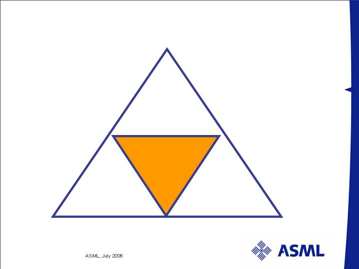
Overlay
Productivity
Defects
Containment
of
water
Minimize
evaporation
Prevent
drying stains
Maximize
scan speed
The immersion challenge triangle
/ Slide 18
hydrophilic
Air curtain allows for high speed scanning for
increased productivity
0
25%
50%
75%
100%
20°
120°
Air Curtain
Productivity
Advantage
Air Curtain OFF
40°
60°
80°
100°
Receding contact angle
Air Curtain ON
Resists & developer
soluble top coats
hydrophobic
solvent soluble
/ Slide 19
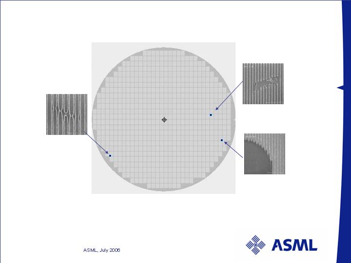
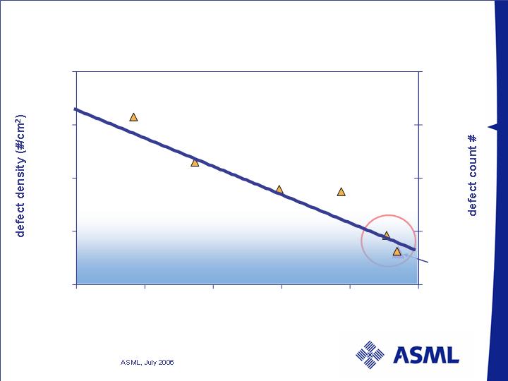
0.006 def/cm2 ( 3 defects )
XT:1400i @ 500-mm/s speed: Only 3 immersion
defects
100-nm L/S
In cooperation with TEL
/ Slide 20
Scanner:
ASML XT:1400i
@ 500mm/sec
Track
TEL Lithius i+
Process:
BARC AZ-Clariant 1CD5
Resist TOK TArF6011
TC TOK TILC031
Inspection:
KLA-Tencor 2365
TSMC
Single Digit Defect Zone
0.001
0.01
0.1
1
10
Nov-04
Feb-05
May-05
Sep-05
Dec-05
Mar-06
1
10
100
1000
10000
Defect levels comparable to ‘dry’ systems
demonstrated
/ Slide 21
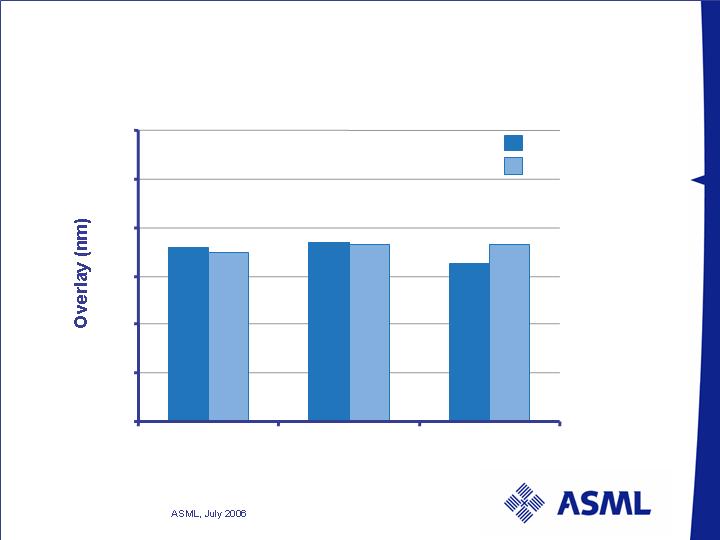
Immersion dual-stage overlay of 7 nm
Day 1
Day 2
Day 3
0
2
4
6
8
10
12
X
Y
XT:1700i
/ Slide 22
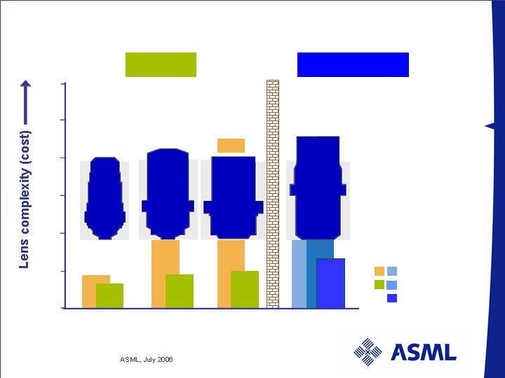
Lens design and manufacturing innovation for max NA
8
0
2
4
6
10
12
0.75
2001
0.85
2003
0.93
2005
1.2
2006
NA
Year
Water Immersion
0
2
4
6
10
12
Dry (air)
1100
1200
1400
Catadioptric design
Geometric scaling
Dioptric designs
Lens Design
1700i
/ Slide 23
Benefits of in-line catadioptric lens design
Source: Carl Zeiss SMT patent applications
Catadioptric
Folded Designs
In-line
Dioptric
Single barrel design provides mechanical stability & ease of adjustment
Low angles of incidence on mirrors for polarization control and transmission
Fewer optical elements resulting in lower cost, lens heating and flare
/ Slide 24
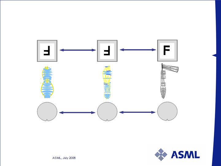
No mask Image flip! Reticle compatibility
Benefits of in-line catadioptric lens design
-
In- Line catadioptric
even # mirrors
Refractive
Lenses
F
F
Reticle
compatibility
-
even # mirrors
Refractive
Lenses
Reticle
compatibility
Folded catadiotric
F
Reticle
uneven # mirrors
Reticle
incompatibility
/ Slide 25
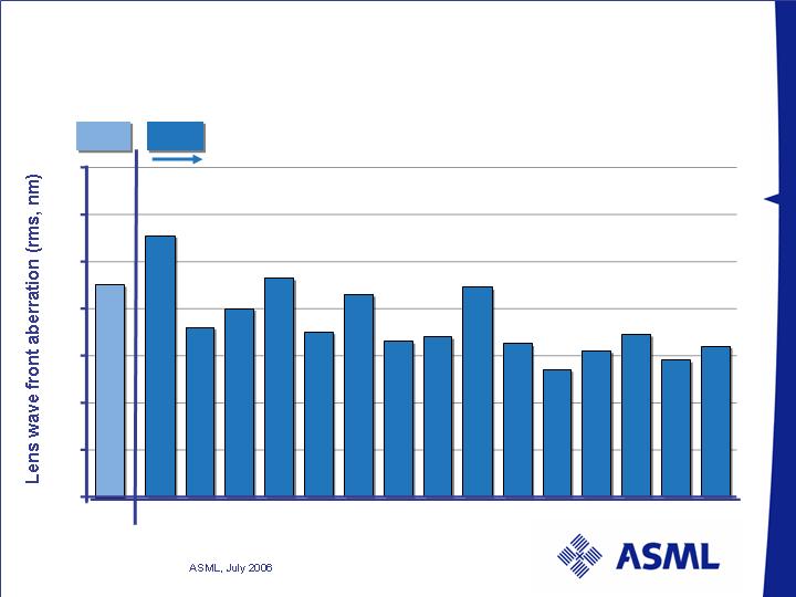
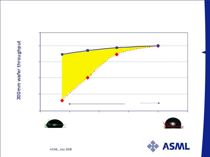
In-line catadioptric lens is manufacturing and
performance proven
0
0.2
0.4
0.6
0.8
1.0
1.2
1.4
Mean
1700i
1
1400
2
3
4
5
6
7
8
9
10
11
12
13
14
15
Lens Production
/ Slide 26
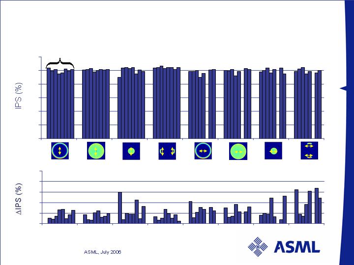
Excellent polarization performance at multiple systems
88
90
92
94
96
98
100
0
0.5
1
1.5
2
2.5
Polarization Purity
Multiple
Systems
Polarization Purity variation across field
/ Slide 27
Polarized imaging down to 42 nm
550-mm/s scan speed
/ Slide 28
Data proven excellent CD control across wafer
550-mm/s scan speed
Using reticle error and process correction
Full Wafer CDU 1.4 nm
45-nm Dense Lines
Intra Field CDU 0.9 nm
45-nm Dense Lines
/ Slide 29
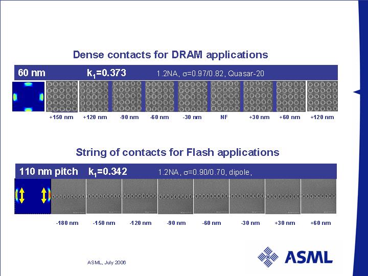
Imaging of challenging contact layers
/ Slide 30

Contents
Inspiration: Market drivers
Immersion: Ramping to volume production
Innovation: Pushing ArF Lithography
to 40 nm and below
/ Slide 31
“40nm and below”
Highest NA
ArFi lens: 1.35 NA
Improved Overlay
6 nm
Highest Productivity
Fastest Scanning Stages:
131 wph
@ 125 exposures / wafer
TWINSCAN XT:1900i provides the best resolution,
productivity and overlay
/ Slide 32
Milestones in immersion leadership
/ Slide 33
Lens design and manufacturing innovation for max NA
8
0
2
4
6
10
12
0.75
2001
0.85
2003
0.93
2005
1.2
2006
NA
Year
Water Immersion
0
2
4
6
10
12
Dry (air)
2007
1.35
1100
1200
1400
1700i
1900i
/ Slide 34

ASML mask and system enhancements extend
lithography to the limit of k 1
Offline Dual stage wafer
height mapping
Focus Dry, Expose Wet
Mask enhancement
techniques &
optimization software
DoseMapper for optimum
CD Uniformity
Application specific
lens setup
Flexible off-axis &
polarized illumination
In-built wave-front, polarization
and pupil metrology
Illumination source
optimization & software
+
=
/ Slide 35
Polarized dipole
Illumination
1:1 Dense Lines
using 6% att-PSM
Image in film calc.
+/-3% dose error
+/-10% CD spec
XT:1900i is designed for 40-nm volume production
0.0
0.1
0.2
0.3
0.4
0.5
0.6
0.7
0.8
35
40
45
50
55
60
Resolution half-pitch [nm]
XT:1900i
1.35 NA
XT:1400i
0.93 NA
XT:1700i
1.2 NA
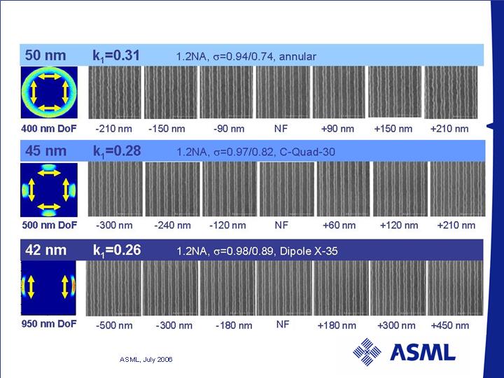
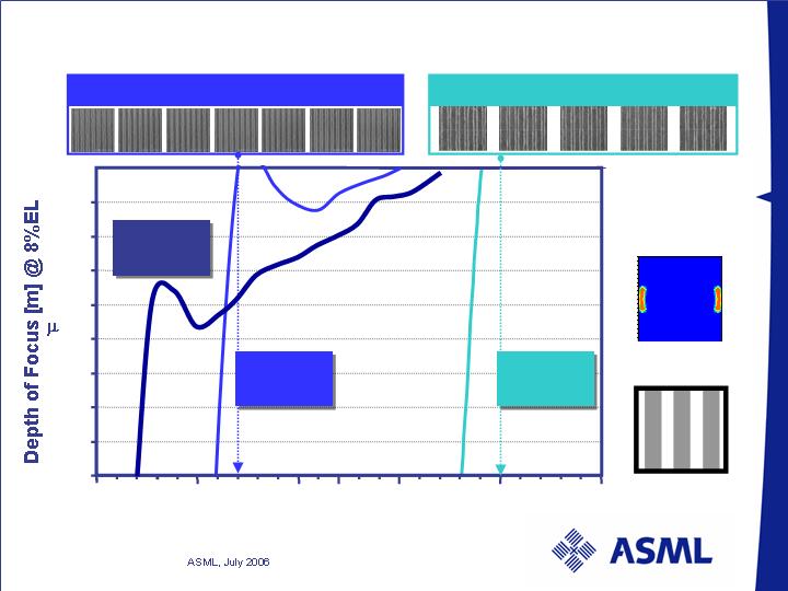
XT:1400i : 1100 nm DoF @ 55 nm
XT:1700i : 950 nm DoF @ 42 nm
/ Slide 36
ASML products enable shrink
10
12
200
100
80
60
40
Logic
DRAM
NAND
11
07
09
08
04
06
05
01
03
02
00
ASML Product
Introduction
XT:1400
XT:1700i
AT:1200
AT:850
XT:1900i
/ Slide 37
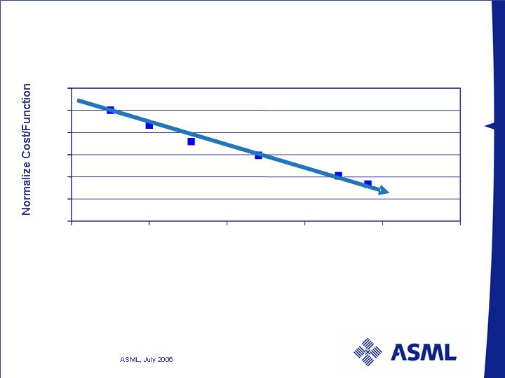
Cost per function continues downward trend
ASML aligns to customer value drivers by
delivering lower cost per function
850
KrF
1150
ArF
1250
ArF
1400
ArF
1700
ArFi
1900
ArFi
0.00
0.20
0.40
0.60
0.80
1.00
1.20
2000
2002
2004
2006
2008
2010
0.00
0.20
0.40
0.60
0.80
1.00
1.20
2000
2002
2004
2006
2008
2010
850
KrF
1150
ArF
1250
ArF
1400
ArF
1700
ArFi
1900
ArFi
/ Slide 38
TWINSCAN XT:1900i: 40 nm and below
Volume production at 40 nm and below
Fifth generation immersion tool on TWINSCAN dual
wafer stage platform with improved overlay 6 nm and
131 W/hr productivity
Proven catadioptric lens concept with manufacturing
and volume ramp up capability
Enabling our customer to continue aggressive device
shrinks for increased functionality at lower costs
/ Slide 39

Extending water-based immersion towards the limit
ASML offers full suite of TWINSCAN immersion products
with resolutions from 65- to 40-nm and below
20 immersion systems shipped to customer sites on three
continents
TWINSCAN XT:1900i most advanced immersion system
of the industry and ready for shipment by mid 2007
TWINSCAN customer acceptance: 500 system shipments
/ Slide 40

Commitment