
Privileged Environment for Leadership
ISS Europe 2006
Eric Meurice, President and CEO, ASML
Exhibit 99.4
Outline
Roadmap for Leadership in Technology
AND Affordability
Successful delivery of the Roadmap
/ Slide 2
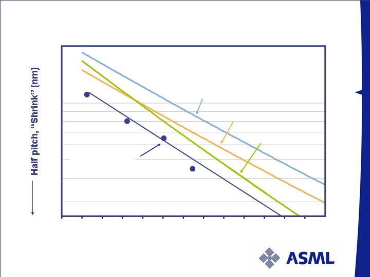
Customers’ appetite for shrink continues unabated
ahead of Moore’s law
10
12
200
100
80
60
40
Logic
DRAM
NAND
11
07
09
08
04
06
05
01
03
02
00
ASML Product
Introduction
XT:1400
XT:1700i
AT:1200
AT:850
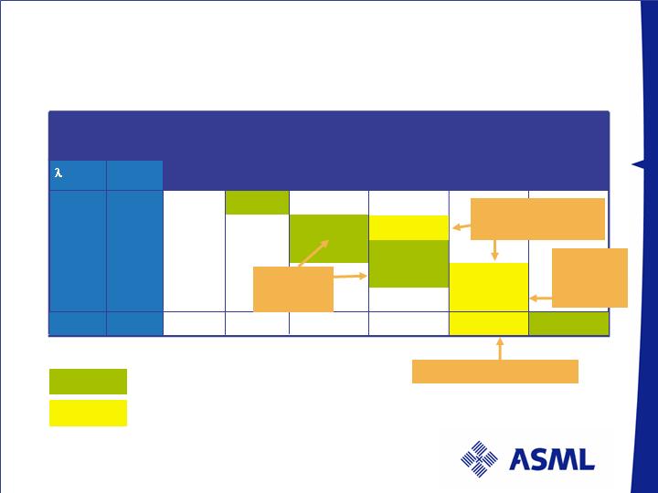
ASML committed to cost effective litho solutions to meet needs
/ Slide 3
0.85
0.93
1.20
1.35
1.50
NA
0.25
0.22
0.31
0.28
0.40
0.31
193
(nm)
Year
22
2011
32
2009
45
2007
65
2005
90
2003
110
2001
Half pitch (nm)
0.25
0.41
0.59
13.5
likely
opportunity
0.40
Infrastructure challenge
Pitch relaxation or
double patterning
0.22
Fluid/
material
challenge
Likely technology roadmap to meet customer
roadmap
Low k1
challenge
k1 = (half pitch) * NA / wavelength
Most aggressive k1 in production today is 0.28/0.3
Physical limit single exposure is 0.25
/ Slide 4
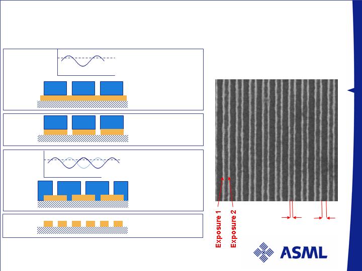
Double patterning as a bridge solution to EUV?
Si
Nitride HM
Resist
Int.
Exposure 1
& development
Transfer to
hard mask
Int.
Exposure 2
& development
Transfer to
hard mask
80-nm pitch
k1=0.2, ArF, 0.93 NA
Space 1 = Space 2
- Overlay
/ Slide 5
ArF Immersion extension with High Index?
>>2010
>2010
2009
2007
Estimated Timing
18%
13%
4%
Shrink
33
35
39
40
Minimum Resolution,
k 1=0.28
1.65
1.55
1.4
1.35
Max NA (0.95 * RImin)
1.9
1.9
1.57
1.57
Refractive Index
New
Material
New
Material
Current
Current
Glass
>1.8
1.65
1.65
1.44
Refractive Index
New
Available
Available
Water
Fluid
/ Slide 6
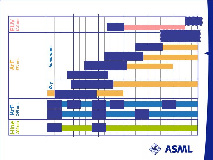
2004
2005
2006
2007
2008
2009
120-90 nm
180-130 nm
280 nm
80-70 nm
65 nm
70 nm
45 nm
65 nm
40 nm
4X0
7X0
8X0
450
760
860
1250 NA=0.85
1250i NA=0.85
1400i NA=0.93
1700i NA=1.2
NA >1.3X
45 nm
32 nm
ADT
32 nm
NA >1.5
or Dbl Pattern
EUV
870
ASML’s product roadmap to meet customer roadmap challenge
875
1400 NA=0.93
/ Slide 7
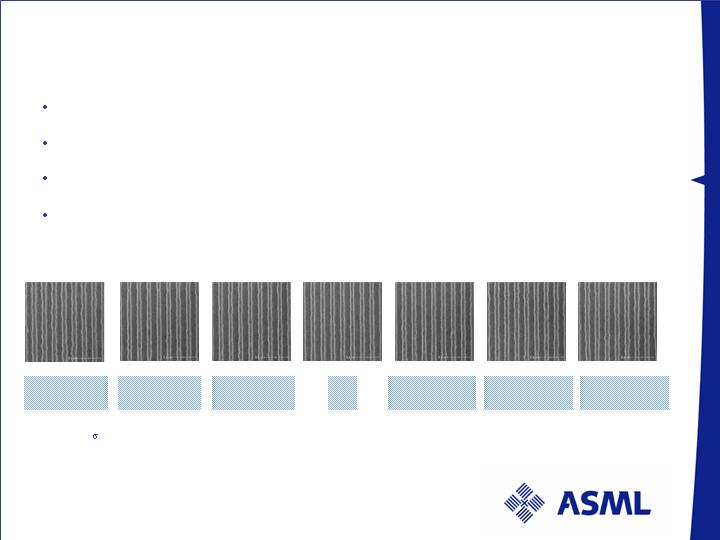
TWINSCAN XT:1700i: 42-nm images
1.2 NA: highest in the industry
Catadioptric lens design
30% increase in resolution
Volume production at 45 nm
-300 nm
NF
+300 nm
+450 nm
-500 nm
-180 nm
+180 nm
42-nm/84-nm pitch,
NA=1.2, =0.89/0.98 dipole X-35, polarized
Resist: 120-nm FFEM RK2101
BARC: 42-nm 1C5D
Top Coat: 140-nm TILC019
Tool: XT:1700Fi
/ Slide 8
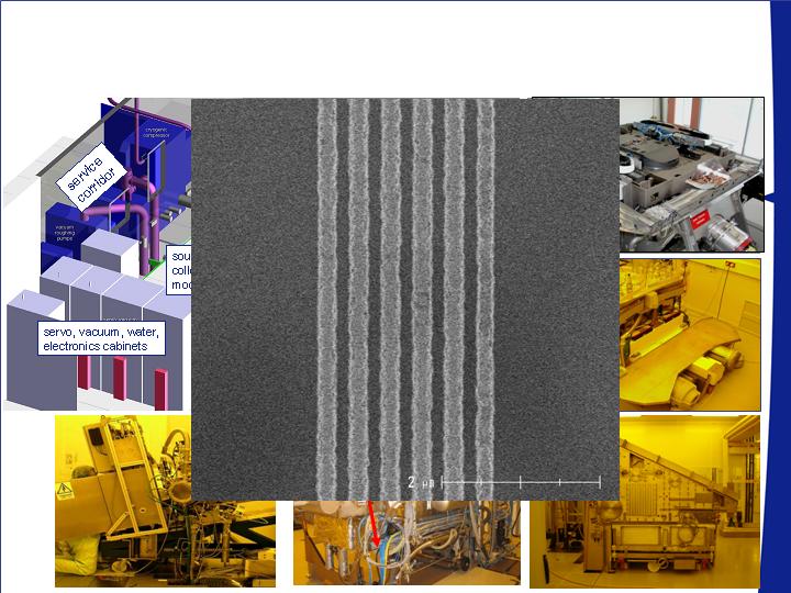
Integration 2 EUV tools in progress: shipment H1 2006
40 nm L&S, > 10 W/hr, 0.25 NA, 13 nm, 26 mm field
AD1
AD2
First
200-nm
image
/ Slide 9
Litho cost places EUV favorably vs. other technologies
XT:850
XT:1250
XT:1400
XT:1700
EUV
ArFi DP
ArFi hi
EUV
ArFi DP
130
90
65
45
32
32
32
22
22
2001
2003
2005
2007
2009
2009
2011
2011
2011
Mask cost high
Mask cost low
Litho cost
Source: ASML
/ Slide 10
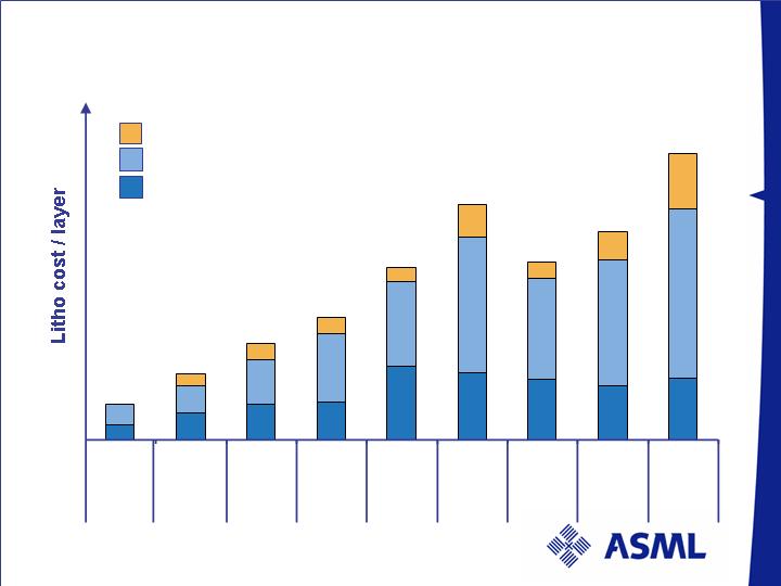
Cost per layer =
Cost
Productivity
Improvements in productivity, cost
effective lens, and equipment
design deliver lower cost per layer
ASML solution to increasing technology costs: continuous
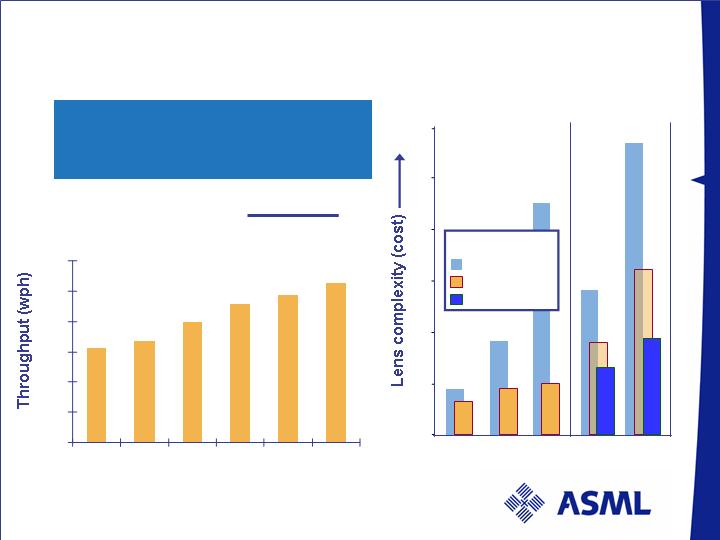
productivity improvement of TWINSCAN & advanced lens solutions
0
25
50
75
100
125
150
2001
2002
2003
2004
2005
2006
0
2
4
6
8
10
12
0.75
2001
0.85
2003
0.93
2005
1.2
2006
>1.3
2007
NA :
Year :
Dry
Wet
Catadioptric
Geometric
Dioptric
Lens Design
Source:ASML
/ Slide 11
0.0
0.1
0.2
0.3
0.4
0.5
0.6
0.7
0.8
0.9
1.0
2000
2002
2004
2006
2008
2010
2012
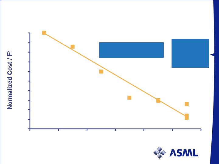
Lithography cost Affordability:
Cost per minimum Feature 2 continuous shrink
32 nm
ArFi DP
32 nm
EUV
32 nm
ArFi hi
22 nm
ArFi DP
22 nm
EUV
Hi index ArFi
challenged
in timing &
extensibility
CoO of EUV & DP ArFi
support 2 year roadmap
XT:1700i
45 nm
1.2 NA ArFi
AT:850
130 nm
0.8 NA KrF
XT:1250
90 nm
0.85 NA ArF
Source: ASML
XT:1400
65 nm
0.93 NA ArF
/ Slide 12

Outline
Roadmap for Leadership in Technology
AND Affordability
Successful delivery of the Roadmap
/ Slide 13
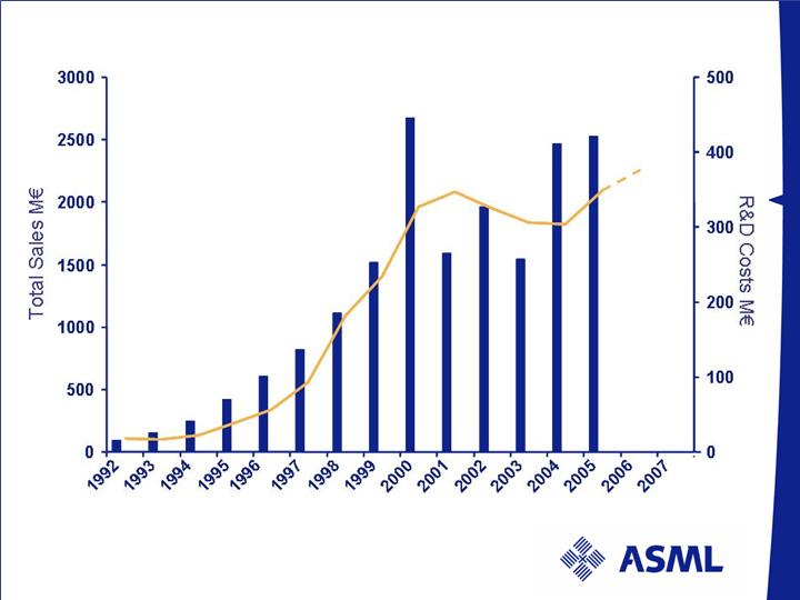
ASML IC Litho R&D costs versus total sales
R&D costs exclude settlement
with Nikon Corp. in 2004 and reflect costs for continuing operations
/ Slide 14
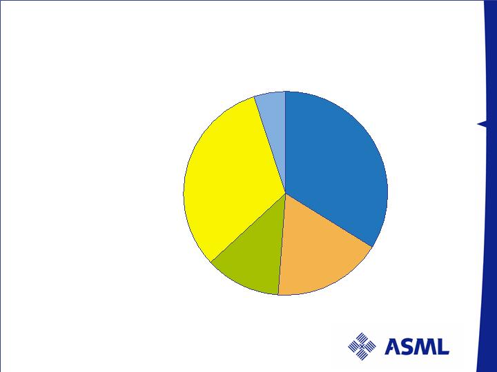
ASML leveraged knowledge base
Payroll resources ~34%
Contractor/outsourcing ~17%
(Work that can be done more
efficiently outside)
Technology buy ~12%
(Bringing external expertise in-house)
Supplier R&D ~32%
Customer network/
applications partners ~5%
/ Slide 15
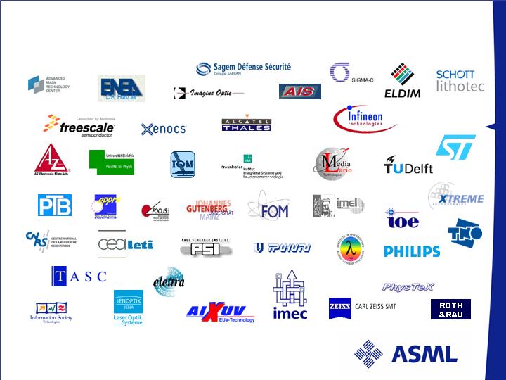
EUV partnering: Europe is active
/ Slide 16
ASML litho specialist pool: large and highly
specialized
ASML employs 2800 in Europe
R&D:
1048 payroll
640 contracted
153
PhD/Dr.
Plus supplier base and technology network:
another 10,000 jobs
/ Slide 17
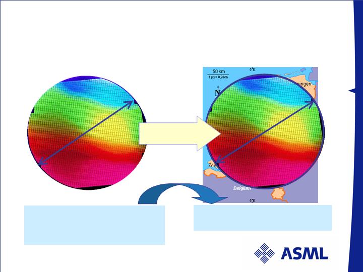
Minimum feature size 50 nm
Positional accuracy +/- 10 nm
Note: 1nm = 1/1,000,000 mm
300 mm
300-mm wafer
ASML system deliverables: Enlarge a wafer 1 million
times and print the Netherlands in 30 seconds
300 km
The Netherlands
Source: ASML
300 km
X1 million
Corresponds to 5 cm
Positional accuracy +/- 1.0 cm
/ Slide 18
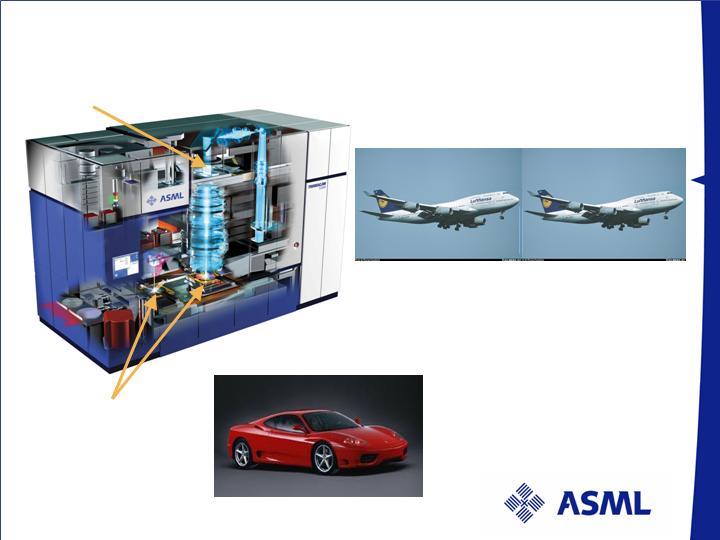
ASML system deliverables
Two TWINSCANTM scanner
stages operate at a speed of
550 mm/s with an accuracy
of 2 nanometer,
which compares to two 747
jumbo jets flying at 1000 km/hr
the exact same route to an
accuracy of 0.001 millimeter
The reticle stage accelerates
from 0 to 100 km/hour in 1.6 seconds,
leaving every sports car behind.
Reticle stage
Wafer stages
/ Slide 19

Conclusions
A clearer, more secured roadmap ahead of
Moore’s Law
A roadmap continuing to deliver reduced cost by
function – litho is affordable
Success hinging on critical mass investment by
ASML and the industry
/ Slide 20
Commitment